Visible to Intel only — GUID: xde1714403150352
Ixiasoft
Answers to Top FAQs
1. Introduction to Quartus® Prime Pro Edition
2. Quick Start Steps
3. Planning FPGA Design for RTL Flow
4. Working With Intel® FPGA IP Cores
5. Creating a New FPGA Design Project
6. Migrate Your FPGA Design Project
7. Managing Quartus® Prime Projects
8. Next Steps After Getting Started
A. Using the Design Space Explorer II
B. Document Revision History for Quartus® Prime Pro Edition User Guide Getting Started
4.1. IP Catalog and Parameter Editor
4.2. Installing and Licensing Intel® FPGA IP Cores
4.3. IP General Settings
4.4. Adding IP to IP Catalog
4.5. Best Practices for Intel® FPGA IP
4.6. Specifying the IP Parameters and Options ( Quartus® Prime Pro Edition)
4.7. IP Core Generation Output ( Quartus® Prime Pro Edition)
4.8. Scripting IP Core Generation
4.9. Modifying an IP Variation
4.10. Upgrading IP Cores
4.11. Simulating Intel® FPGA IP Cores
4.12. Generating Simulation Files for Platform Designer Systems and IP Variants
4.13. Synthesizing IP Cores in Other EDA Tools
4.14. Instantiating IP Cores in HDL
4.15. Support for the IEEE 1735 Encryption Standard
4.16. Related Trainings and Resources
6.1.2.1. Modifying Entity Name Assignments
6.1.2.2. Resolving Timing Constraint Entity Names
6.1.2.3. Verifying Generated Node Name Assignments
6.1.2.4. Replace Logic Lock (Standard) Regions
6.1.2.5. Modifying Signal Tap Logic Analyzer Files
6.1.2.6. Removing References to .qip Files
6.1.2.7. Removing Unsupported Feature Assignments
6.1.4.1. Verifying Verilog Compilation Unit
6.1.4.2. Updating Entity Auto-Discovery
6.1.4.3. Ensuring Distinct VHDL Namespace for Each Library
6.1.4.4. Removing Unsupported Parameter Passing
6.1.4.5. Removing Unsized Constant from WYSIWYG Instantiation
6.1.4.6. Removing Non-Standard Pragmas
6.1.4.7. Declaring Objects Before Initial Values
6.1.4.8. Confining SystemVerilog Features to SystemVerilog Files
6.1.4.9. Avoiding Assignment Mixing in Always Blocks
6.1.4.10. Avoiding Unconnected, Non-Existent Ports
6.1.4.11. Avoiding Invalid Parameter Ranges
6.1.4.12. Updating Verilog HDL and VHDL Type Mapping
6.1.4.13. Converting Symbolic BDF Files to Acceptable File Formats
7.1. Viewing Basic Project Information
7.2. Managing Project Settings
7.3. Viewing Parameter Settings From the Project Navigator
7.4. Managing Logic Design Files
7.5. Managing Timing Constraints
7.6. Integrating Other EDA Tools
7.7. Exporting Compilation Results
7.8. Archiving Projects
7.9. Command-Line Interface
7.10. Related Trainings
7.7.1. Exporting a Version-Compatible Compilation Database
7.7.2. Importing a Version-Compatible Compilation Database
7.7.3. Creating a Design Partition
7.7.4. Exporting a Design Partition
7.7.5. Reusing a Design Partition
7.7.6. Viewing Quartus Database File Information
7.7.7. Clearing Compilation Results
Visible to Intel only — GUID: xde1714403150352
Ixiasoft
2. Quick Start Steps
Follow these steps to get started with Quartus® Prime Pro Edition software:
Figure 3. Quartus® Prime Pro Edition Software Quick Start Steps
Use the following links to get started with the Quartus® Prime Pro Edition software:
| Step | Useful Links | |
|---|---|---|
| Determine the System Requirements | Verify hardware and software requirements and review Quartus® Prime Pro Edition software release notes. | |
| Download the software | Download the latest Quartus® Prime Pro Edition software. | |
| Install the software | Install the latest Quartus® Prime Pro Edition software. | |
| Generate 90-days Fixed-node License | Generate 90- days free license in Intel® FPGA Self-Service Licensing Center (SSLC). | |
| Start the software | On Windows: Use one of the following options:
On Linux:
|
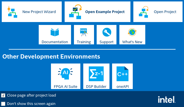
Starting the Quartus® Prime Software |
| Set up the generated license in the Quartus® Prime Pro Edition software | In the Quartus® Prime Pro Edition software, click Tools > License Setup, browse and select the license file, and click OK. | |
| Quartus® Prime Software Home Page | Main page of the Quartus® Prime software. |
|
| Plan FPGA Design for RTL Flow | Planning for RTL flow is an essential step for advanced FPGA design. Determining your design priorities early on helps you to choose the best device, tools, features, and methodologies for your design. | Plan FPGA Design for RTL Flow |
| Create your FPGA project | The Quartus® Prime software makes it easy for you to quickly setup a new FPGA design project. | Creating a New FPGA Design Project |
| Get Started with FPGA Designing | Use one of the following options:
|
|
| Set Up Your Project | Use one of the following options:
|
|
| Manage Your Project | Organize and manage the elements of your design within a project to encapsulate information about your design files, hierarchy, libraries, constraints, and project settings. | Managing Quartus Prime Projects |
| Constrain Your Design | Assign design elements to I/O pins, and apply appropriate timing constraints to correctly optimize fitting and analyze timing for the design. | Managing Device I/O Pins |
| Compile Your Design | Run the compiler to synthesize logic design files considering the device characteristics and design constraints. | Using the Compilation Dashboard |
| Close Timing on Your Design | Perform timing analysis of a compiled design using the Timing Analyzer, which determines the timing relationships that your design must meet to function correctly and according to the timing specifications. | Timing Analyzer Quick-Start Tutorial: Quartus® Prime Pro Edition Quartus® Prime Pro Edition User Guide: Timing Analyzer |
| Configure Your Design on the Board | Once your design meets the specifications, you can create programming files and upload those files to the device. | Basic Device Configuration Steps |

