Visible to Intel only — GUID: osa1651157203680
Ixiasoft
Visible to Intel only — GUID: osa1651157203680
Ixiasoft
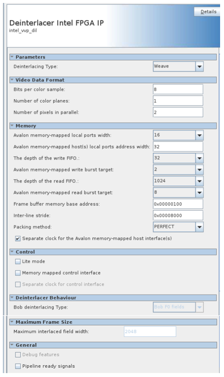
23.2. Deinterlacer Parameters
| Parameter | Values | Description |
|---|---|---|
| Parameters | ||
| Deinterlacing mode | Bob or Weave | Select bob or weave deinterlacer. |
| Video Data Format | ||
| Bits per color sample | 8 to 16 | Select the number of bits per color sample. |
| Number of color planes | 1 to 4 | Select the number of color planes per pixel. |
| Number of pixels in parallel | 1 to 8 | Select the number of pixels in parallel. |
| Memory 58 | ||
| Avalon memory- mapped host(s) local ports width | 16, 32, 64, 128, 256, 512, 1024 | Select in bits the width of the Avalon memory-mapped host read and write ports. |
| Avalon memory- mapped host(s) local ports address width | 8 to 32 | Select in bits the width of the Avalon memory-mapped host read and write ports. It must be sufficient to fully address the last buffer. |
| The depth of the write FIFO | 32, 64, 128, 256, 512, 1024, 2048 | Select the depth of the write FIFO buffer. Each FIFO buffer entry holds one word the width of the specified Avalon memory-mapped local port width. You must specify a FIFO depth of at least twice the specified burst target so that at least 2 bursts can be held at any one time. Increase the FIFO depth to improve resilience to latency on the Avalon memory-mapped bus. |
| Avalon memory- mapped write burst target | 2,4,8,16,32,64 | Select the burst target for writes. Longer bursts provide more efficiency on the bus but require more local storage in the write FIFO buffer. |
| The depth of the read FIFO | 32,64,128,256,512,1024,2048 | Specify the depth of the read FIFO buffer. Each FIFO buffer entry holds one word the width of the specified Avalon memory-mapped local port width. You must specify a FIFO depth of at least twice the specified burst target so that at least 2 bursts can be held at any one time. Increase the FIFO depth to improve resilience to latency on the Avalon memory-mapped bus. |
| Avalon memory- mapped read burst target | 2,4,8,16,32,64 | Select the burst target for reads. Longer bursts provide more efficiency on the bus but require more local storage in the read FIFO buffer. |
| Field memory base address | 0x0000_0000 – 0x7FFF_FFFF | Select the base address for the field buffer to store field 0 or field 1. |
| Interline stride | Depends on video frame format and maximum frame width. | Set a stride (in bytes) large enough to separate lines of the specified maximum width. The GUI gives an error if the stride is too low. |
| Packing method | Perfect, color or pixel | Perfect packing minimizes memory footprint of stored fields but increases complexity and therefore size of the field buffer slightly. Color packing leaves spaces in memory between colors if colors do not pack into memory words exactly. Pixel packing leaves spaces in memory between pixels if pixels do not pack into memory words exactly. |
| Separate clock for the Avalon memory- mapped host interface(s) | On or off | A separate clock allows the control and data portions of the field buffer to run at their maximum clock frequencies. Turn on separate clocks for highest performance. |
| Control | ||
| Lite mode | On or off | Turn on to operate the deinterlacer in lite mode. |
| Memory-mapped control interface | On or off | Turn on to read frame statistics and turn the deinterlacer on and off using an Avalon memory-mapped interface. The memory-mapped control interface is mandatory in lite mode. |
| Separate clock for control interface | On or off | Turn on for a separate clock for the control interface. |
| Deinterlacer Behavior 59 | ||
| Bob deinterlacing mode | DEINTERLACE_F0_ONLY, DEINTERLACE_F1_ONLY, DEINTERLACE_F0_AND_F1 |
Select to drop off F0 or F1 input fields. |
| Maximum Frame Size | ||
| Maximum field width | 32 to 16384 | Select the maximum field width to determine the size of the line buffer. Set this parameter to the line length of the widest fields you want to deinterlace. Progressive frames of any size pass through unchanged. |
| General | ||
| Debug features | On or off | Turn on to enable debug features (not applicable for lite mode). |
| Pipeline ready signals | On or off | Turn on to add extra pipeline registers to the AXI4-S tready signals |
| Use FIFO | On or off | Add optional FIFO buffer. |

The figure shows the weave deinterlacing, where the IP drops or deinterlaces interlaced fields. The IP passes all progressive frames through. For incoming F1 and F0, the weave deinterlacer deinterlaces or drops the fields based on the nibble values. For more information on nibble, refer to the Intel FPGA Streaming Video Protocol Specification.