Visible to Intel only — GUID: bmq1703181403311
Ixiasoft
Visible to Intel only — GUID: bmq1703181403311
Ixiasoft
B.1.3. PIO Design Example Testbench
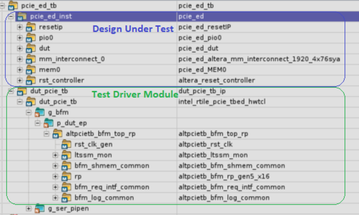
The figure below shows the PIO design example simulation design hierarchy. The tests for the PIO design example are defined with the apps_type_hwtcl parameter set to 3. The tests run under this parameter value are defined in ebfm_cfg_rp_ep_rootport, find_mem_bar and downstream_loop.

- Issue a memory write command to write a single dword of data into the on-chip memory behind the Endpoint.
- Issue a memory read command to read back data from the on-chip memory.
- Compare the read data with the write data. If they match, the test counts this as a Pass.
- Repeat Steps 1, 2 and 3 for 10 iterations.
The first memory write takes place around 219 us. It is followed by a memory read at the Avalon® -ST RX interface of the Hard IP for PCIe. The Completion TLP appears shortly after the memory read request at the Avalon® -ST TX interface.