A newer version of this document is available. Customers should click here to go to the newest version.
Visible to Intel only — GUID: hzy1630477484163
Ixiasoft
1. About the Nios® V Embedded Processor
2. Nios® V Processor Hardware System Design with Intel® Quartus® Prime Software and Platform Designer
3. Nios® V Processor Software System Design
4. Nios® V Processor Configuration and Booting Solutions
5. Nios® V Processor - Using the MicroC/TCP-IP Stack
6. Nios® V Processor Debugging, Verifying, and Simulating
7. Nios® V Processor — Remote System Update
8. Nios® V Embedded Processor Design Handbook Archives
9. Document Revision History for the Nios® V Embedded Processor Design Handbook
4.1. Introduction
4.2. Linking Applications
4.3. Nios® V Processor Booting Methods
4.4. Introduction to Nios® V Processor Booting Methods
4.5. Nios® V Processor Booting from Configuration QSPI Flash
4.6. Nios V Processor Booting from On-Chip Memory (OCRAM)
4.7. Summary of Nios® V Processor Vector Configuration and BSP Settings
6.4.1. Prerequisites
6.4.2. Setting Up and Generating Your Simulation Environment in Platform Designer
6.4.3. Creating Nios V Processor Software
6.4.4. Generating Memory Initialization File
6.4.5. Generating System Simulation Files
6.4.6. Running Simulation in the QuestaSim Simulator Using Command Line
Visible to Intel only — GUID: hzy1630477484163
Ixiasoft
1.4.2.1.2. Generating the Nios® V/m Processor Example Design System in Platform Designer
To generate the Nios® V/m processor example design system in Platform Designer, perform the following steps:
- Open the top.qpf project file in Intel® Quartus® Prime software. Go to Tool > Platform Designer.
- Create a new Platform Designer system and name it as sys.qsys.
- Save the system.
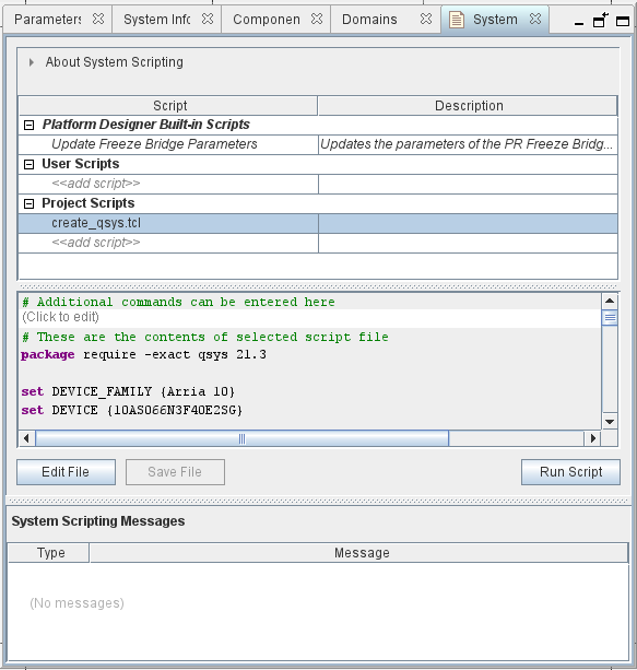
- In the Platform Designer, go to View > System Scripting. The System Scripting window appears.
- Under the Project Scripts, add and click Run Script to run the create_qsys.tcl script.
Figure 3. System Scripting window

- The generated Platform Designer system consist of a clock bridge, reset bridge, Nios® V/m processor, on-chip memory and JTAG UART IP.
- Click Generate HDL to generate the system HDL.
Note: To target another Intel FPGA device other than the Arria 10 SoC Development Kit, update the FAMILY, DEVICE, and clock pin assignments in the top.qsf file.
- Click Processing > Start Compilation to perform a full hardware compilation and generate the .sof file.