Visible to Intel only — GUID: upy1651192660278
Ixiasoft
1. About the R-Tile Avalon® Streaming Intel® FPGA IP for PCI Express
2. IP Architecture and Functional Description
3. Advanced Features
4. Interfaces
5. Parameters
6. Troubleshooting/Debugging
7. R-Tile Avalon® Streaming Intel® FPGA IP for PCI Express* User Guide Archives
8. Document Revision History for the R-Tile Avalon® Streaming Intel FPGA IP for PCI Express User Guide
A. Configuration Space Registers
B. Root Port Enumeration
C. Implementation of Address Translation Services (ATS) in Endpoint Mode
D. Packets Forwarded to the User Application in TLP Bypass Mode
E. Margin Masks for the R-Tile Avalon Streaming Intel FPGA IP for PCI Express
3.2.2.5.1. VirtIO Common Configuration Capability Register (Address: 0x012)
3.2.2.5.2. VirtIO Common Configuration BAR Indicator Register (Address: 0x013)
3.2.2.5.3. VirtIO Common Configuration BAR Offset Register (Address: 0x014)
3.2.2.5.4. VirtIO Common Configuration Structure Length Register (Address 0x015)
3.2.2.5.5. VirtIO Notifications Capability Register (Address: 0x016)
3.2.2.5.6. VirtIO Notifications BAR Indicator Register (Address: 0x017)
3.2.2.5.7. VirtIO Notifications BAR Offset Register (Address: 0x018)
3.2.2.5.8. VirtIO Notifications Structure Length Register (Address: 0x019)
3.2.2.5.9. VirtIO Notifications Notify Off Multiplier Register (Address: 0x01A)
3.2.2.5.10. VirtIO ISR Status Capability Register (Address: 0x02F)
3.2.2.5.11. VirtIO ISR Status BAR Indicator Register (Address: 0x030)
3.2.2.5.12. VirtIO ISR Status BAR Offset Register (Address: 0x031)
3.2.2.5.13. VirtIO ISR Status Structure Length Register (Address: 0x032)
3.2.2.5.14. VirtIO Device Specific Capability Register (Address: 0x033)
3.2.2.5.15. VirtIO Device Specific BAR Indicator Register (Address: 0x034)
3.2.2.5.16. VirtIO Device Specific BAR Offset Register (Address 0x035)
3.2.2.5.17. VirtIO Device Specific Structure Length Register (Address: 0x036)
3.2.2.5.18. VirtIO PCI Configuration Access Capability Register (Address: 0x037)
3.2.2.5.19. VirtIO PCI Configuration Access BAR Indicator Register (Address: 0x038)
3.2.2.5.20. VirtIO PCI Configuration Access BAR Offset Register (Address: 0x039)
3.2.2.5.21. VirtIO PCI Configuration Access Structure Length Register (Address: 0x03A)
3.2.2.5.22. VirtIO PCI Configuration Access Data Register (Address: 0x03B)
4.3.1. Avalon® Streaming Interface
4.3.2. Precision Time Measurement (PTM) Interface (Endpoint Only)
4.3.3. Interrupt Interface
4.3.4. Hard IP Reconfiguration Interface
4.3.5. Error Interface
4.3.6. Completion Timeout Interface
4.3.7. Configuration Intercept Interface
4.3.8. Power Management Interface
4.3.9. Hard IP Status Interface
4.3.10. Page Request Services (PRS) Interface (Endpoint Only)
4.3.11. Function-Level Reset (FLR) Interface (Endpoint Only)
4.3.12. SR-IOV VF Error Flag Interface (Endpoint Only)
4.3.13. General Purpose VSEC Interface
5.2.3.1. Device Capabilities
5.2.3.2. VirtIO Parameters
5.2.3.3. Link Capabilities
5.2.3.4. Legacy Interrupt Pin Register
5.2.3.5. MSI Capabilities
5.2.3.6. MSI-X Capabilities
5.2.3.7. Slot Capabilities
5.2.3.8. Latency Tolerance Reporting (LTR)
5.2.3.9. Process Address Space ID (PASID)
5.2.3.10. Device Serial Number Capability
5.2.3.11. Page Request Service (PRS)
5.2.3.12. Access Control Service (ACS)
5.2.3.13. Power Management
5.2.3.14. Vendor Specific Extended Capability (VSEC) Registers
5.2.3.15. TLP Processing Hints (TPH)
5.2.3.16. Address Translation Services (ATS) Capabilities
5.2.3.17. Precision Time Measurement (PTM)
Visible to Intel only — GUID: upy1651192660278
Ixiasoft
6.6.4.2. Event Counters
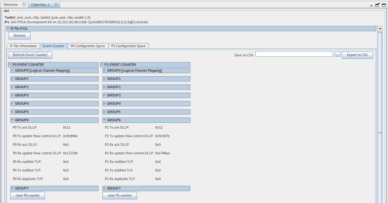
This tab allows you to read the events occurring at the link level, such as the number of received errors, framing errors, etc. for each port. You can use the Clear PX counter button at the end of each event counter list to reset these counters. Also, please note that:
- All the information is read-only.
- The per-lane related counters correspond to the logical lanes.
- Use the Refresh Event Counter button to read the event counters' registers.
| Group | Counter Size | Description |
|---|---|---|
| 0 | 4 bits | Elastic Buffer (EBUF) Overflow |
| Elastic Buffer (EBUF) Under-run | ||
| Decode Error | ||
| Running Disparity Error | ||
| Gen3 (G3) SKP OS Parity Error | ||
| Gen3 - Gen5 (G3-G5) SYNC Header Error | ||
| Rx Valid deassert w/o EIOS | ||
| CTL SKP OS Parity Error | ||
| 1st Retimer Parity Error | ||
| 2nd Retimer Parity Error | ||
| Gen4 (G4) Margin CRC & Parity Error | ||
| 1 | 8 bits | Detect Electrical Idle (EI) Inferred |
| Receiver Error | ||
| Rx Recovery Request | ||
| N_FTS Timeout | ||
| Gen3 (G3) Framing Error | ||
| Deskew Error | ||
| 2 | 8 bits | Bad TLP |
| LCRC Error | ||
| Bad DLLP | ||
| Replay Number Rollover | ||
| Replay Timeout | ||
| Rx Nak DLLP | ||
| Tx Nak DLLP | ||
| Retry TLP | ||
| 3 | 8 bits | Flow Control (FC) Timeout |
| Poisoned TLP | ||
| ECRC Error | ||
| Unsupported Request | ||
| Completer Abort | ||
| Completion Timeout | ||
| 4 | 4 bits | Elastic Buffer (EBUF) SKP Addition |
| Elastic Buffer (EBUF) SKP Deletion | ||
| 5 | 32 bits | L0 to Recovery |
| L1 to Recovery | ||
| ASPM L1 Reject | ||
| L1 Entry | ||
| L2 Entry | ||
| Speed Change | ||
| Link Width Change | ||
| 6 | 32 bits | Tx Ack DLLP |
| Tx Update Flow Control (FC) DLLP | ||
| Rx Ack DLLP | ||
| Rx Update Flow Control (FC) DLLP | ||
| Rx Nullified TLP | ||
| Tx Nullified TLP | ||
| Rx Duplicate TLP | ||
| 7 | 32 bits | Tx Memory Write |
| Tx Memory Read TLP | ||
| Tx Configuration Write TLP | ||
| Tx Configuration Read TLP | ||
| Tx IO Write TLP | ||
| Tx IO Read TLP | ||
| Tx Completion without Data TLP | ||
| Tx Completion with Data TLP | ||
| Tx Message TLP (VC Only) TLP | ||
| Tx Atomic TLP | ||
| Tx TLP with Prefix | ||
| Rx Memory Write TLP | ||
| Rx Memory Read TLP | ||
| Rx Configuration Write TLP | ||
| Rx Configuration Read TLP | ||
| Rx IO Write TLP | ||
| Rx IO Read TLP | ||
| Rx Completion without Data TLP | ||
| Rx Completion with Data TLP | ||
| Rx Message TLP (VC Only) TLP | ||
| Rx Atomic TLP | ||
| Rx TLP with Prefix |
Figure 64. Event Counters Tab

