Visible to Intel only — GUID: mdx1638186989111
Ixiasoft
1. About the Video and Vision Processing Suite
2. Getting Started with the Video and Vision Processing IPs
3. Video and Vision Processing IPs Functional Description
4. Video and Vision Processing IP Interfaces
5. Video and Vision Processing IP Registers
6. Video and Vision Processing IPs Software Programming Model
7. Protocol Converter Intel® FPGA IP
8. 1D LUT Intel® FPGA IP
9. 3D LUT Intel® FPGA IP
10. Adaptive Noise Reduction Intel® FPGA IP
11. Advanced Test Pattern Generator Intel® FPGA IP
12. AXI-Stream Broadcaster Intel® FPGA IP
13. Bits per Color Sample Adapter Intel® FPGA IP
14. Black Level Correction Intel® FPGA IP
15. Black Level Statistics Intel® FPGA IP
16. Chroma Key Intel® FPGA IP
17. Chroma Resampler Intel® FPGA IP
18. Clipper Intel® FPGA IP
19. Clocked Video Input Intel® FPGA IP
20. Clocked Video to Full-Raster Converter Intel® FPGA IP
21. Clocked Video Output Intel® FPGA IP
22. Color Plane Manager Intel® FPGA IP
23. Color Space Converter Intel® FPGA IP
24. Defective Pixel Correction Intel® FPGA IP
25. Deinterlacer Intel® FPGA IP
26. Demosaic Intel® FPGA IP
27. FIR Filter Intel® FPGA IP
28. Frame Cleaner Intel® FPGA IP
29. Full-Raster to Clocked Video Converter Intel® FPGA IP
30. Full-Raster to Streaming Converter Intel® FPGA IP
31. Genlock Controller Intel® FPGA IP
32. Generic Crosspoint Intel® FPGA IP
33. Genlock Signal Router Intel® FPGA IP
34. Guard Bands Intel® FPGA IP
35. Histogram Statistics Intel® FPGA IP
36. Interlacer Intel® FPGA IP
37. Mixer Intel® FPGA IP
38. Pixels in Parallel Converter Intel® FPGA IP
39. Scaler Intel® FPGA IP
40. Stream Cleaner Intel® FPGA IP
41. Switch Intel® FPGA IP
42. Text Box Intel® FPGA IP
43. Tone Mapping Operator Intel® FPGA IP
44. Test Pattern Generator Intel® FPGA IP
45. Unsharp Mask Intel® FPGA IP
46. Video and Vision Monitor Intel FPGA IP
47. Video Frame Buffer Intel® FPGA IP
48. Video Frame Reader Intel FPGA IP
49. Video Frame Writer Intel FPGA IP
50. Video Streaming FIFO Intel® FPGA IP
51. Video Timing Generator Intel® FPGA IP
52. Vignette Correction Intel® FPGA IP
53. Warp Intel® FPGA IP
54. White Balance Correction Intel® FPGA IP
55. White Balance Statistics Intel® FPGA IP
56. Design Security
57. Document Revision History for Video and Vision Processing Suite User Guide
31.4.1. Achieving Genlock Controller Free Running (for Initialization or from Lock to Reference Clock N)
31.4.2. Locking to Reference Clock N (from Genlock Controller IP free running)
31.4.3. Setting the VCXO hold over
31.4.4. Restarting the Genlock Controller IP
31.4.5. Locking to Reference Clock N New (from Locking to Reference Clock N Old)
31.4.6. Changing to Reference Clock or VCXO Base Frequencies (switch between p50 and p59.94 video formats and vice-versa)
31.4.7. Disturbing a Reference Clock (a cable pull)
Visible to Intel only — GUID: mdx1638186989111
Ixiasoft
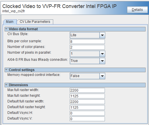
20.2. Clocked Video to Full-Raster Converter Parameters
| Parameter | Values | Description |
|---|---|---|
| Video Data Format | ||
| CV Bus Style | Lite, CVI or CVO | Select which sideband signals the IP drives, and which signals are available in Platform Designer. A second tab allows you to parameterize the CV bus style. |
| Bits per color sample | 6 to 16 | Number of bits per color sample. |
| Number of color planes | 1 to 4 | Number of color planes in a pixel. |
| Number of pixels in parallel | 1, 2, 4 or 8 | Number of pixels transmitted every clock. |
| AXI4S FR Bus has tReady connection | True or False | Select true so the streaming full-raster interface contains the AXI4-S tReady signal. Select false to remove, the tReady signal. |
| Control Settings | ||
| Memory-mapped control interface | True or False | Select True to turn on the CPU interface and associated signals. Select False to remove the CPU interface and for all the CPU registers to use default values. |
| Separate clock for control interface | True or False | Select True to include the signal cpu_clock in Platform Designer. It is asynchronous to the video domain. Select False so the CPU interface uses the signal vid_clock. |
| Dimensions | ||
| Max full-raster width | 1 to 65535 | The maximum width of raster that this IP passes. |
| Max full-raster height | 1 to 65535 | The maximum height of raster this IP passes. |
| Default full-raster width | 1 to 65535 | The width of the raster. The CPU can override this value. |
| Default full-raster height | 1 to 65535 | The height of the raster. The CPU can override this value. |
| Default Vsync H | 1 to 65535 | The default pixel position of the rising edge of the vertical timing signal (vsync or vblank) The CPU can override this value. |
| Default Vsync V | 1 to 65535 | The default line where the rising edge of the vertical timing signal (vsync or vblank) occurs. The CPU can override this value. |
Figure 49. Main Parameters
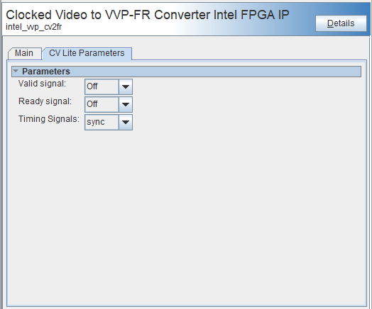
| Parameter | Values | Description |
|---|---|---|
| Parameters | ||
| Valid signal | On or off | When you select Lite the IP includes an optional data valid input signal, cv_vid_in_valid. Turn on to turn on this input in the IP. Platform Designer includes or removes the signal from the cv_vid_in conduit as appropriate. |
| Ready signal | On or off | When you select Lite the IP includes an optional data ready output signal, cv_vid_in_ready. Turn on to turn on this output in the IP. Platform Designer includes or removes the signal from the cv_vid_in conduit as appropriate. |
| Timing Signals | sync, blank, or both | Select which timing are available. Platform Designer includes or removes the signals from the cv_vid_in conduit as appropriate |
Figure 50. CV Lite Parameters
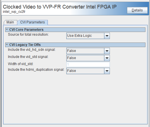
| Parameters | Values | Description |
|---|---|---|
| CVI Core Parameters | ||
| Source for total resolution | Use Extra Logic or Use External Signals | The IP requires the height and width of the raster. Determine this information using additional logic within the IP, or get the information from optional input signals. This parameter selects the source for the raster dimensions. Platform Designer includes or removes the signals from the cv_vid_in conduit as appropriate |
| CVI Legacy Tie Offs | ||
| Include the vid_hd_sdn signal | True or False | Select True to add this signal to the cv_vid_in conduit. The signal has no function within the IP and is included for connectivity within Platform Designer. |
| Include the vid_std signal | True or False | Select True to add this signal to the cv_vid_in conduit. The signal has no function within the IP and is included for connectivity within Platform Designer. |
| Width of vid_std | 1 to 16 | The width of the vid_std signal. |
| Include the hdmi_duplication signal | True or False | Select True to add this signal to the cv_vid_in conduit. The signal has no function within the IP and is included for connectivity within Platform Designer. |
Figure 51. CVI Parameters
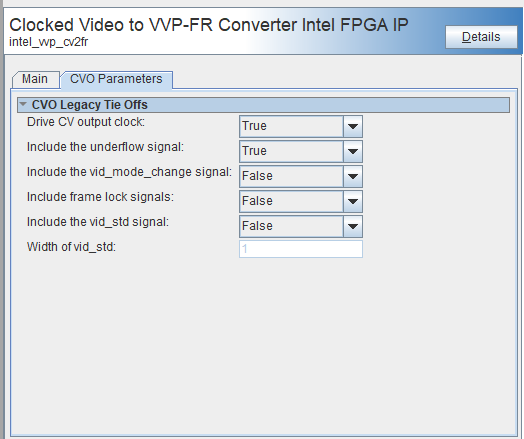
| Parameters | Values | Description |
|---|---|---|
| CVO Legacy Tie Offs | ||
| Drive CV Output Clock | True or False | Select True to add this signal to the cv_vid_in conduit. The signal has no function within the IP and is included for connectivity within Platform Designer. |
| Include the underflow signal | True or False | Select True to add this signal to the cv_vid_in conduit. The signal has no function within the IP and is included for connectivity within Platform Designer. |
| Include the vid_mode_change signal | True or False | Select True to add this signal to the cv_vid_in conduit. The signal has no function within the IP and is included for connectivity within Platform Designer. |
| Include the frame lock signals | True or False | Select True to add this signal to the cv_vid_in conduit. The signal has no function within the IP and is included for connectivity within Platform Designer. |
| Include the vid_std signal | True or False | Select True to add this signal to the cv_vid_in conduit. The signal has no function within the IP and is included for connectivity within Platform Designer. |
| Width of vid_std | 1 to 16 | Select the width of the vid_std signal. |
Figure 52. CVO Parameters