2.5. Generating the Synthesizable High Bandwidth Memory (HBM2) Interface Intel FPGA IP for High Efficiency
To generate the synthesizable design example with high efficiency in the HBM2 interface and measure the traffic efficiency using the In-System Sources and Probes (ISSP) Editor, follow these steps.
- On the Controller tab, deselect the option. The Reorder Buffer rearranges the read data in the order of the issued requests.
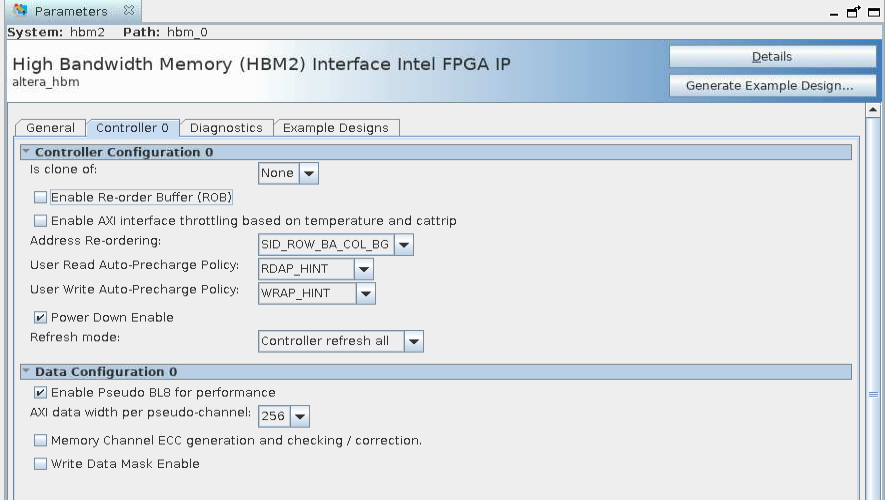
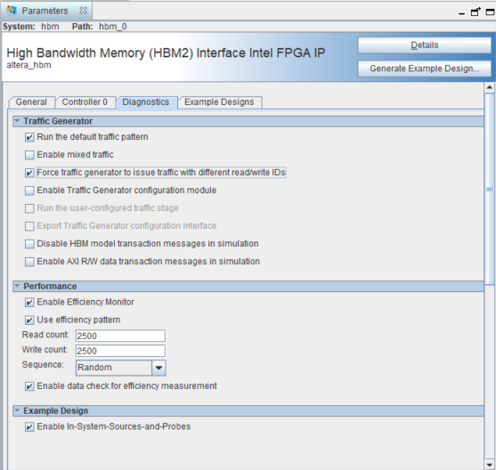
- On the Diagnostics tab, select . Also, select .
- Set both the Read Count and Write Count values to at least 2500, and select the Sequential option for data traffic Sequence. (Alternatively, if you want to measure the efficiency for traffic with random addresses, set the Sequence option to Random.)
- On the Diagnostics tab, select . Also, select . If it is not already checked, check the Enable In-System-Sources-and-Probes checkbox in the Example Design group box.
- Click Generate Example Design at the top-right corner of the parameter editor to generate the synthesizable design example.
- Apply the specific pinout for the development kit and compile the design.
- After the design example is programmed on the circuit board, you can obtain efficiency performance results using the ISSP editor.
- Monitor and ensure transactions have completed as indicated by a 1 on the EFFT probe in the In-System Sources and Probes (ISSP) Editor.
The EFFR 32-bit probe signals can display the value of valid write and read transactions and the total number of active transactions.
The EFFW is a 3-bit input set source input signal which enables output on the EFFR 32-bit probe signals. The following table shows input values for EFFW and the corresponding EFFR counter output values:
Table 3. EFFW Source Value Description of EFFR output (32-bits wide) 3'b 000 Number of valid write data transactions. 3'b 001 Number of valid read data transactions. 3'b 010 Total active transaction count. 3'b 100 Minimum read latency. 3'b 101 Maximum read latency. 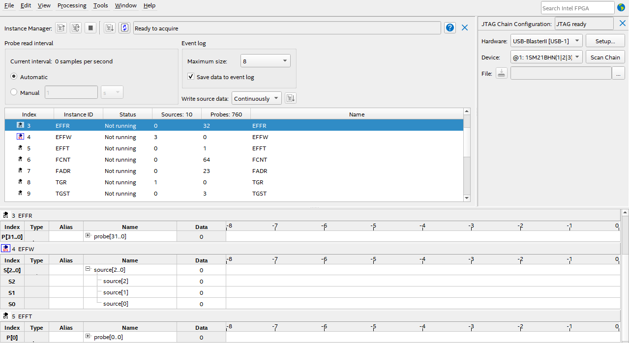
- You can calculate efficiency using the following formula, based on the counter values:
Efficiency=[(Number of Write Data transactions + Number of Read Data transactions accepted by HBM2 controller) ÷ (total active transaction count) × [(core clock frequency) × 2) ÷ (HBM2 interface frequency)] × 100.For example, given the following values:
- Write data transactions: 5000
- Read data transactions: 5000
- Total active transactions: 10358
- Core clock frequency: 250 MHz
- HBM2 interface frequency: 600 MHz
Efficiency = [(5000+5000)÷(10358)×(250)×2÷600]×100=80.5%
- The traffic generator runs with the efficiency pattern for one test loop by default. To reinitiate the test, reset the HBM2 design example using the ISSP editor. You can use the RSTN signal to reset the HBM2 design example by writing a 0 and then a 1.
Note: For additional information on changing the test duration and traffic pattern for the Intel® Stratix® 10 HBM2 traffic generator, refer to the Intel® Stratix® 10 High Bandwidth Memory (HBM2) Traffic Generator video, available here: https://www.youtube.com/watch?v=XLfw12VCm0U.