Visible to Intel only — GUID: ykp1538666715038
Ixiasoft
1. About the High Bandwidth Memory (HBM2) Interface Intel® FPGA IP
2. High Bandwidth Memory (HBM2) Interface Intel FPGA IP Design Example Quick Start Guide
3. High Bandwidth Memory (HBM2) Interface Intel FPGA IP Design Example Description
4. High Bandwidth Memory (HBM2) Interface Intel® FPGA IP Design Example User Guide Archives
5. Document Revision History for the High Bandwidth Memory (HBM2) Interface Intel® FPGA IP Design Example User Guide
2.1. Creating an Intel® Quartus® Prime Project for Your HBM2 System
2.2. Configuring the High Bandwidth Memory (HBM2) Interface Intel FPGA IP
2.3. IP Parameter Editor Pro Guidelines for High Bandwidth Memory (HBM2) Interface Intel FPGA IP
2.4. Generating the Synthesizable High Bandwidth Memory (HBM2) Interface Intel FPGA IP Design Example
2.5. Generating the Synthesizable High Bandwidth Memory (HBM2) Interface Intel FPGA IP for High Efficiency
2.6. Generating the High Bandwidth Memory (HBM2) Interface Intel FPGA IP Design Example for Simulation
2.7. Regenerating the High Bandwidth Memory (HBM2) Interface Intel FPGA IP Design Example After Modification
Visible to Intel only — GUID: ykp1538666715038
Ixiasoft
2.4. Generating the Synthesizable High Bandwidth Memory (HBM2) Interface Intel FPGA IP Design Example
For the Intel® Stratix® 10 MX development kit, you may leave most of the High Bandwidth Memory (HBM2) Interface Intel FPGA IP settings at their default values. To generate the synthesizable design example, follow these additional steps.
- On the Diagnostics tab, select Example Design > Enable In-System-Sources-and-Probes to provide access to the available debugging features integrated in the design example.
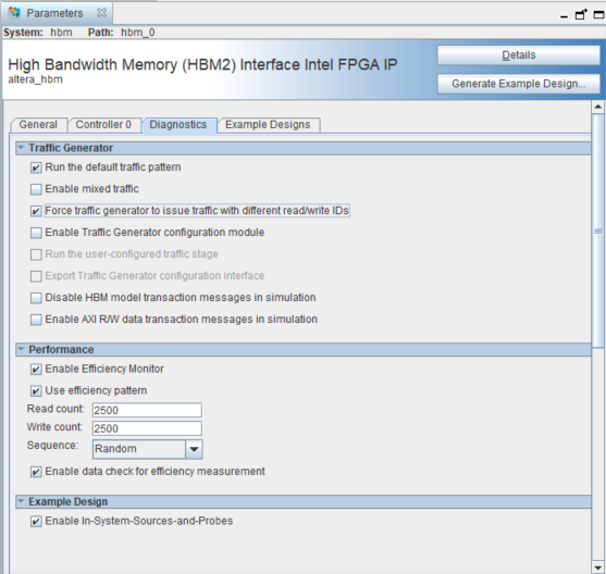
- On the Diagnostics tab, select Performance > Use efficiency pattern to provide high-efficiency concurrent traffic pattern features integrated in the design example. You can configure the different number of read/write transactions, select between sequential or random traffic addressing, and enable or disable the data-matching check. This option also enables the Read command round trip latency feature. Latency is measured from the start of read command valid by the driver, until the response is received.
- If it is not already checked, check the Synthesis checkbox under Example Design Files on the Example Designs tab.
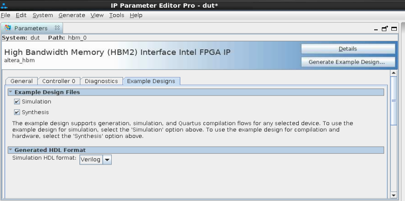 Note: The system enables both the Simulation and Synthesis checkboxes by default.
 - Click File > Save. The system creates and saves the current settings in the user IP variation file (<user instance name>.ip), within the <user project directory> that you specified.
- Click Generate Example Design in the top-right corner of the window.
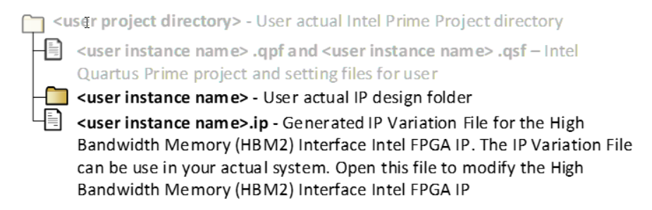
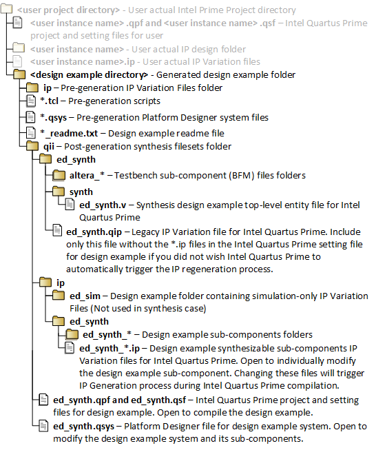
- Specify a directory for the generated design example (<design example directory>) and click OK. The system creates the following design example file sets within the specified directory:
- To exit the IP Parameter Editor Pro window, click File > Exit.