External Memory Interfaces Agilex™ 7 M-Series FPGA IP Design Example User Guide
A newer version of this document is available. Customers should click here to go to the newest version.
Visible to Intel only — GUID: ewo1668274299220
Ixiasoft
Visible to Intel only — GUID: ewo1668274299220
Ixiasoft
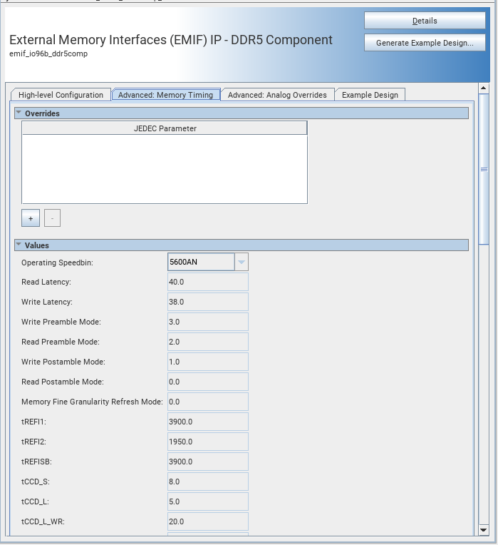
2.2.2. Using Custom Memory Timing and I/O Configuration
To modify the Advanced: Memory timing and Advanced Analog: overrides values, follow these steps:
- In the IP parameter editor, select the Advanced: Memory timing or Advanced Analog: overrides tab.
- In the overrides tab, click the + beneath the JEDEC Parameter box.
Figure 9. Advanced: Memory Timing Tab
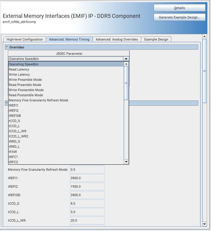
- Click the parameter that appears in the JEDEC Parameter box. A drop-down menu appears. Select the parameter that you want to change.
Figure 10. Drop-down Menu
- In the list under the values section, search for the parameter you want to change and input the value on the field next to it.
Figure 11. Modifying an Advanced Memory Timing Value
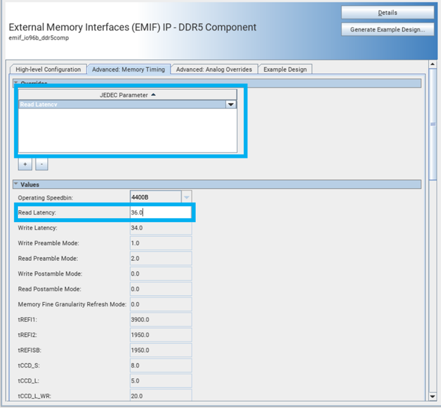
If the specified value is not valid for the parameter, an error message appears, listing the valid values.