Visible to Intel only — GUID: lat1731438788193
Ixiasoft
1. About the External Memory Interfaces Agilex™ 7 M-Series FPGA IP
2. Design Example Quick Start Guide for External Memory Interfaces Agilex™ 7 M-Series FPGA IP
3. Design Example Description for External Memory Interfaces Agilex™ 7 M-Series FPGA IP
4. Document Revision History for External Memory Interfaces Agilex™ 7 M-Series FPGA IP Design Example User Guide
2.1. Creating an EMIF Project
2.2. Generating and Configuring the EMIF IP
2.3. Parameterizing the External Memory Interface for HPS IP
2.4. Configuring DQ Pin Swizzling
2.5. Generating the Synthesizable EMIF Design Example
2.6. Generating the EMIF Design Example for Simulation
2.7. Pin Placement for Agilex™ 7 M-Series EMIF IP
2.8. Compiling the Agilex™ 7 M-Series EMIF Design Example
2.9. Using the EMIF Design Example with the Test Engine IP
2.10. Generating the EMIF Design Example with the Performance Monitor
2.4.1. Example: DQ Pin Swizzling Within DQS group for x32 DDR4 interface
2.4.2. Example: Byte Swizzling for a x32 DDR4 interface, using a memory device of x8 width
2.4.3. Combining Pin and Byte Swizzling
2.4.4. Example: Swizzling for a x32 + ECC interface
2.4.5. Example: Swizzling for a 2Ch x32 + ECC interface
2.4.6. Example: Byte Swizzling for Lockstep Configuration
Visible to Intel only — GUID: lat1731438788193
Ixiasoft
2.3.3. Parameterizing the EMIF IP
Click the EMIF IP that you want to parameterize.
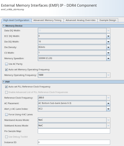
The Parameters tab shows the selected IP and all the parameters that you can change.
Figure 15. External Memory Interfaces Parameters Tab


For more information on the possible parameters and options, refer to the appropriate section describing the selected memory protocol in the External Memory Interfaces Agilex 7 M-Series FPGA IP User Guide. For information on how to parametrize the EMIF IP, refer to Generating and Configuring the EMIF IP, in this document.
Note: In External Memory Interface for HPS IP dual channel configurations, CH0 must be assigned to bank 3D and CH1 to bank 3C.