2.2.1. Agilex™ 7 M-Series EMIF Parameter Editor Guidelines
| Section Name | Guidelines |
|---|---|
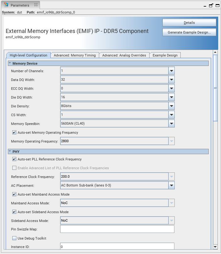
| Memory Device | Ensure that you correctly enter the following parameters:
|
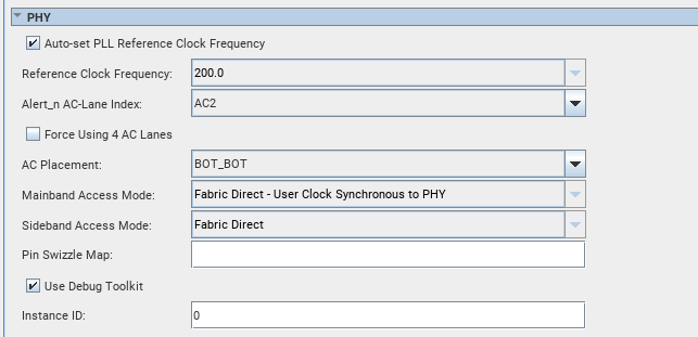
| PHY | Select the desired mode to connect the EMIF IP to user logic:
|
| Advanced: Memory Timing | Allows you to modify the timing values. |
| Advanced: Analog Overrides | Allows you to modify the termination, and VREF settings and drive strengths. |
| Example Design | The Example Design tab lets you select which HDL to use for the top-level files, and which file sets you want the design example to generate. You can also enable the performance monitor and modify the length traffic for the traffic generator. You should make these selections before clicking the Generate Example Design... button. The generated design example is a complete EMIF system consisting of the EMIF IP and a driver that generates random traffic to validate the memory interface. |
When using banks 2A and 2B, select Ch0 Bot Sub-Bank/Ch1 Bot Sub-Bank for the AC placement address and command placement parameter. For banks 3A/3B, 3C/3D, or 2C/2D, there are two options available for the AC placement parameter:
- You must select Ch0 Top Sub-Bank/Ch1 Bot Sub-Bank when placing CH0 address and command pins in the top sub-bank.
- You must select Ch0 Bot Sub-Bank/Ch1 Top Sub-Bank when placing CH0 address and command pins in the bottom sub-bank.

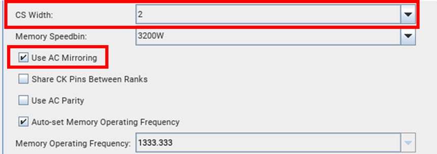
When using DIMMs with dual-die components, ensure that you change the CS Width field to 2 and set the appropriate Command-Address Mirroring value.

For additional information, refer to the DIMM Support subsection of the DDR5 Data Width Mapping topic in the External Memory Interfaces Agilex™ 7 M-Series FPGA IP User Guide.

For detailed information on individual parameters, refer to the appropriate protocol-specific chapter in the External Memory Interfaces Agilex™ 7 M-Series FPGA IP User Guide.