Visible to Intel only — GUID: uci1731437743314
Ixiasoft
1. About the External Memory Interfaces Agilex™ 7 M-Series FPGA IP
2. Design Example Quick Start Guide for External Memory Interfaces Agilex™ 7 M-Series FPGA IP
3. Design Example Description for External Memory Interfaces Agilex™ 7 M-Series FPGA IP
4. Document Revision History for External Memory Interfaces Agilex™ 7 M-Series FPGA IP Design Example User Guide
2.1. Creating an EMIF Project
2.2. Generating and Configuring the EMIF IP
2.3. Parameterizing the External Memory Interface for HPS IP
2.4. Configuring DQ Pin Swizzling
2.5. Generating the Synthesizable EMIF Design Example
2.6. Generating the EMIF Design Example for Simulation
2.7. Pin Placement for Agilex™ 7 M-Series EMIF IP
2.8. Compiling the Agilex™ 7 M-Series EMIF Design Example
2.9. Using the EMIF Design Example with the Test Engine IP
2.10. Generating the EMIF Design Example with the Performance Monitor
2.4.1. Example: DQ Pin Swizzling Within DQS group for x32 DDR4 interface
2.4.2. Example: Byte Swizzling for a x32 DDR4 interface, using a memory device of x8 width
2.4.3. Combining Pin and Byte Swizzling
2.4.4. Example: Swizzling for a x32 + ECC interface
2.4.5. Example: Swizzling for a 2Ch x32 + ECC interface
2.4.6. Example: Byte Swizzling for Lockstep Configuration
Visible to Intel only — GUID: uci1731437743314
Ixiasoft
2.3.1. Parameterization Flow
To parameterize the EMIF for HPS IP, you must first configure the high-level topology by defining the following options:
- Memory protocol for the EMIF IP
- Memory configuration
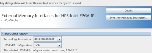
After creating and generating the desired high-level topology, you can set more specific parameters and features of the IP by clicking Dive into Packaged Subsystem. The following figure shows the parameter editor interface.
Figure 13. External Memory Interfaces for HPS IP Parameter Editor

