Visible to Intel only — GUID: wsl1472838893615
Ixiasoft
3.2. Default Switch and Jumper Settings
This topic shows you how to restore the default factory settings and explains their functions.
Figure 3. Default Switch Settings
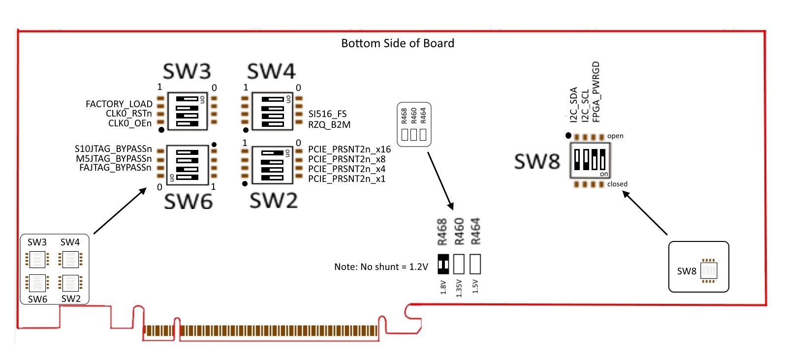
1. Set DIP switch bank (SW2) to match the following table
| Switch | Board Label | Function | Default Position |
|---|---|---|---|
| 1 | x1 | ON for PCIe x1 | OFF |
| 2 | x4 | ON for PCIe x4 | OFF |
| 3 | x8 | ON for PCIe x8 | OFF |
| 4 | x16 | ON for PCIe x16 | ON |
2. If all of the resistors are open, the FMC VCCIO value is 1.2 V. To change that value, add resistors as shown in the following table.
| Board Reference | Board Label | Description |
|---|---|---|
| R460 | 1.35V | 1.35V FMC VCCIO select |
| R464 | 1.5V | 1.5V FMC VCCIO select |
| R468 | 1.8V | 1.8V FMC VCCIO select
Note: A 0 Ohm resistor is installed by default
|
3. Set DIP switch bank (SW6) to match the following table.
| Switch | Board Label | Function | Default Position |
|---|---|---|---|
| 1 | Intel® Stratix® 10 | OFF to enable the Intel® Stratix® 10 in the JTAG chain. ON to bypass the Intel® Stratix® 10 in the JTAG chain. |
OFF |
| 2 | MAX® V | OFF to enable the MAX® V in the JTAG chain. ON to bypass the MAX® V in the JTAG chain. |
OFF |
| 3 | FMC | OFF to enable the FMC Connector in the JTAG chain. ON to bypass the FMC connector in the JTAG chain. |
ON |
4. SW1 DIP Switch Default Settings (Board TOP)
| Switch | Board Label | Function |
|---|---|---|
| 1 | MSEL2 | MSEL [2], MSEL [1] = [0,0] QSPI AS Fast Mode MSEL [2], MSEL [1] = [0,1] QSPI AS Normal Mode MSEL [2], MSEL [1] = [1,0] AVST x16 Mode (Default) MSEL [2], MSEL [1] = [1,1] JTAG Only Mode MSEL [0] is tied to Vcc |
| 2 | MSEL1 |
5. Set DIP switch bank (SW6) to match the following table.
| Switch | Board Label | Function | Default Position |
|---|---|---|---|
| 1 | CLK0_OEn | ON to enable the Si5341A clock device OFF to disable the Si5341A clock device |
ON |
| 2 | CLK0_RSTn | ON to hold the Si5341A clock device in reset OFF to allow the Si5341A clock device to function normally |
OFF |
| 3 | FACTORY_LOAD | ON to load factory image from flash OFF to load user hardware1 from flash |
ON |
| Switch | Board Label | Function | Default Position |
|---|---|---|---|
| 1 | RZQ_B2M | ON for setting RZQ resistor of Bank 2M to 99.17 Ohm OFF for setting RZQ resistor of Bank 2M to 240 Ohm |
OFF |
| 2 | SI516_FS | ON for setting the SDI REFCLK frequency to 148.35 MHz OFF for setting the SDI REFCLK frequency to 148.5 MHz |
OFF |
| Switch | Board Label | Function | Default Position |
|---|---|---|---|
| 1 | I2C_SDA | Connects VRM I2C to MAX® V I2C chain | ON |
| 2 | I2C_SCL | Connects VRM I2C to MAX® V I2C chain | ON |
| 3 | FPGA_PWRGD | Connects LT2987 Power Good to MAX® V | OFF |