Visible to Intel only — GUID: qbq1654715772626
Ixiasoft
1. About the Three-phase Boost Bidirectional AC-DC and LLC DC-DC Converter for Electric Vehicle (EV) Charging Design Example
2. Getting started with the Design Example
3. Functional Description
4. Top-level VHDL Wrapper
5. Simulink Simulation Results
6. Document Revision History for AN 995: Three-phase Boost Bidirectional AC-DC and LLC DC-DC Converter for EV Charging Design Example
Visible to Intel only — GUID: qbq1654715772626
Ixiasoft
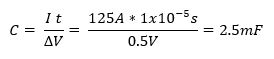
3.2.2.3. Output Capacitor
A subblock emulates the output capacitor or DC-link capacitor, for which you must consider an acceptable output voltage ripple. In the continuous-time domain, you can use standard electronics formula to obtain the capacitor value.
Where:
- ΔV = 0.5 V, which is the acceptable output voltage ripple.
- 1 x 10⁻⁵s is the inverse of the switching frequency.
- 125 A is the maximum output current.
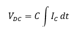
The voltage across the output capacitor (VDC ) is the integral of the current flowing into it as follows:
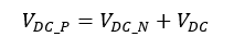
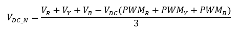
The inductor and switch models calculate the high side current, which is a split between the output capacitor (IC ) and load resistor (ILOAD ). Although VC is controlled to a DC voltage, the voltage on the capacitor terminals is relative to the ground (VDC_P and VDC_N ) switches up and down with the PWM of the switches. The calculation of VDC_P and VDC_N depends on the state of the PWM signals (0 or 1).
Then, calculate VDC_P using: