3.2.4. LLC DC-DC Converter
The LLC DC-DC converter in the Three-phase Boost Bidirectional AC-DC and LLC DC-DC Converter for EV Charging design example takes a DC input and feeds it into a H-bridge switching network, which produces a square wave.
This square wave passes into an LLC resonant circuit - capacitor and transformer. The transformer provides isolation as well as a step-up or down function, and the resonant circuit filters out harmonics. The diode bridge rectifies the alternating output of the transformer back into a DC output. You control the H bridge switches by varying the switching frequency. The duty cycle is fixed at 50%. The switching frequency sets the gain of the resonant circuit. The PI controller produces a proportional gain of 1200 and an integral gain of 105.
DC-DC Converter Controller
A PI controller, which controls the frequency of a pulse generator, controls the LLC DC-DC converter. These pulses turn the bridge switches of the power electronics on and off.
Figure 23. DC-DC Converter Controller Implemented in Simulink with HDL coder blocks
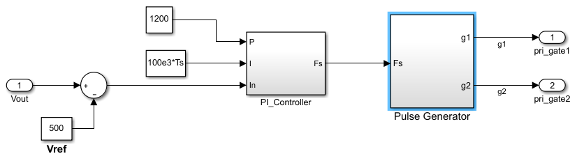
Figure 24. LLC Resonant Tank Frequency ResponseThe figure shows by changing the switching frequency relative to the LLC tank's resonant frequency, you control the gain of the converter along the curve. The PI controller is limited to a range comprising the negative slope of the resonance (the right hand side of the curve).
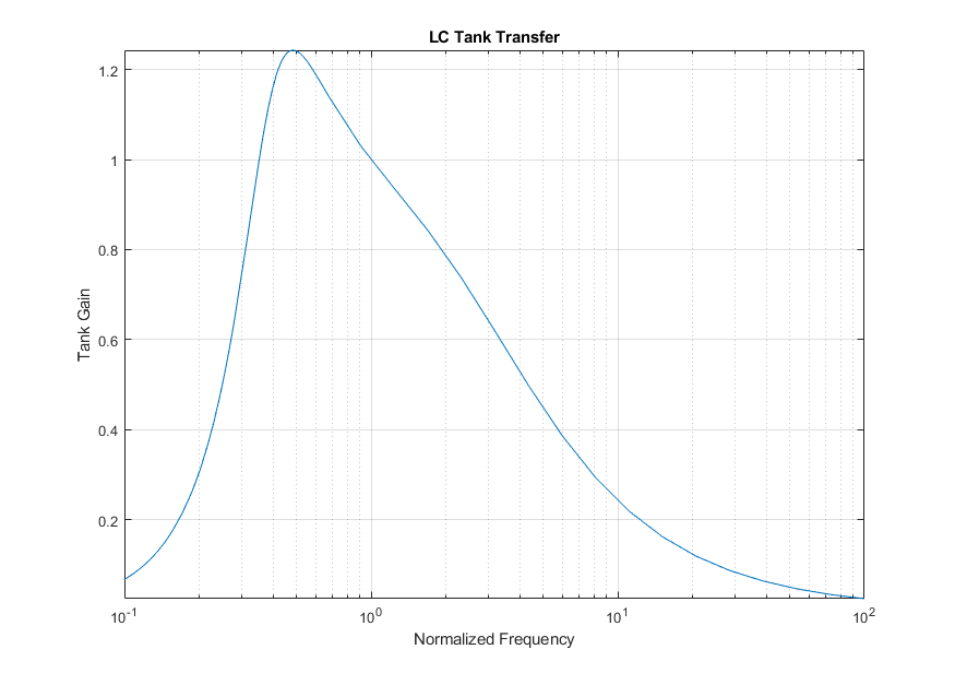
The actual resonant frequency of the LLC tank is 91.4 kHz and the PI controller is limited to 60 kHz to 10 MHz.
Power Electronics
| Component | Value | Unit | |
|---|---|---|---|
| Transformer | Winding turns ratio | 5:8 | |
| Primary inductance | 2.02 | µH | |
| Secondary inductance | 1.16 | µH | |
| Magnetizing inductance | 963 | µH | |
| Resonant capacitor | 1.5 | µF | |
| Output capacitor | 100 | µF | |
Figure 25. Power Electronics Implemented in Simulink with HDL coder blocks
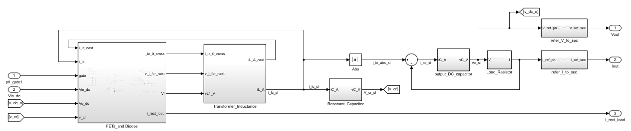
In the model, the capacitors are simple integrators, integrating current to calculate the voltage produces across the terminals. In this model, the transformer is a single series inductance that is a combination of the primary and secondary inductance. The magnetizing inductance is negligible. You calculate the voltages and currents with reference to the primary side of the transformer. The model scales the final output voltage and current by the transformer turns ratio (refer_V_to_sec and refer_I_to_sec blocks). The input switch and output diode bridges produce four states for the circuit with regard to the transformer inductance voltage.
V L = ±V i ±V o - V cr
You determine the polarity of Vi (input voltage) and Vo (output voltage) by the gate switch from the control block and direction of current respectively. Vcr is the voltage across the resonant capacitor. In this model, the transformer integrates the voltage you apply across the terminals to calculate the current through it, with several additions to the model. A look-ahead calculation predicts the current for the next sampling period to predict when the transformer secondary current that flows through the diode bridge changes direction.
During the single sample period when the diode bridge current reverses, the true inductor voltage calculation is more complicated than other sampling periods. For the first part of the sample period, you determine the inductor voltage by applying the output voltage in one polarity but the reverse polarity for the remainder of the sample period. You need to calculate the proportion of the sampling period that the current is flowing in each direction, which involves a mathematical division and therefore a lot of FPGA logic.
One alternative solution is to greatly increase the sampling rate but is not practical to synthesize and run in real-time in the FPGA. However, a sufficiently accurate alternative is to calculate the inductor voltage as if the current was flowing in one direction for the entire sampling period, then again for the opposite current direction and use the mean of the two inductor voltage results. This average is sufficiently accurate and minimizes the FPGA logic.
The FETs and diodes block determines when the diode current reverses and in combination with the input switch control calculates the corresponding transformer inductor voltage.