Visible to Intel only — GUID: ece1693106431408
Ixiasoft
Visible to Intel only — GUID: ece1693106431408
Ixiasoft
7.3.7.3. Routing Guidelines for DDR5 RDIMM, UDIMM, SODIMM and LRDIMM Configurations
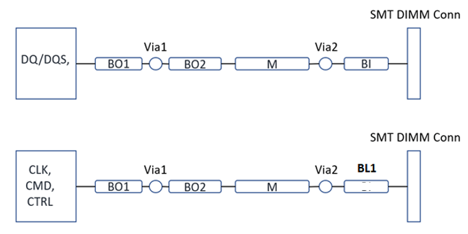
The following figure shows DDR5 1 x DIMM per channel topology. A maximum of two transition vias are allowed for high performance.

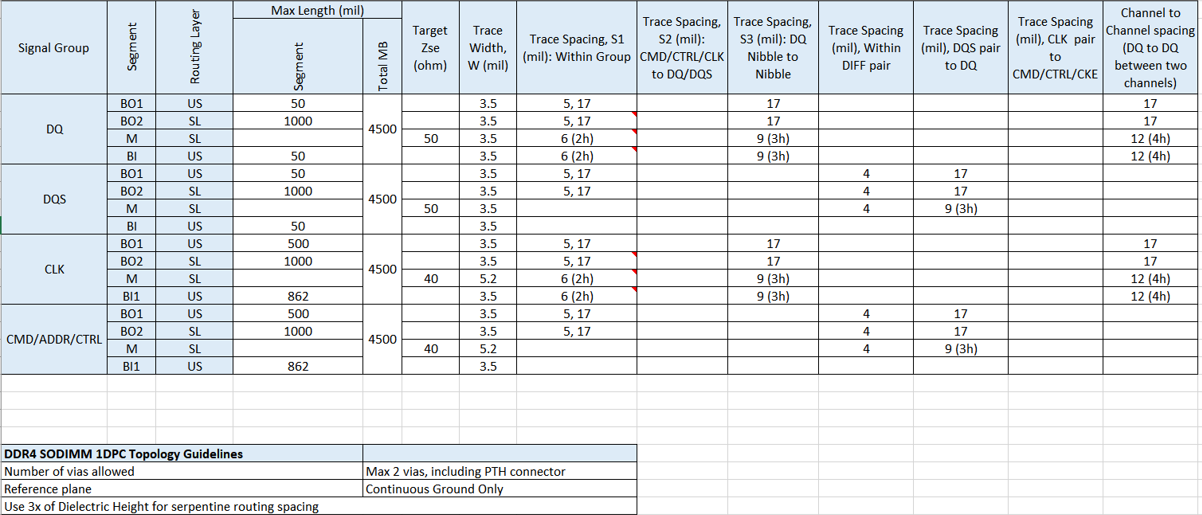
The following table shows physical trace segment routing guidelines, including the target impedance of routing for each signal and the minimum space between signal traces on the same layer. The column trace widths (in mil) and minimum space between traces (in mil) are based on a Intel board design stackup; however, the PCB designer must meet the impedance target criteria. The h in the routing guideline stands for the minimum substrate height between the signal layer and reference plane. Ensure that you follow the trace-to-trace-edge gap/space criteria in the guideline, based on “h” in various stackups.

|
Reset signal routing design also follows the command, address, and control (CMD/ADD/CTRL) routing design. Maintain the space from the Reset signal to other signals on the same layer (edge to edge) at least 5x h. There is no requirement to have skew matching between Reset and CLK signals.
Skew matching for a DDR interface consists of both package routing skew and PCB physical routing skew. You must maintain skew matching of CA and CTRL with respect to the clock signals to ensure that signals at the receiver are correctly sampled. There is also a skew matching requirement for DQ and DQS within a byte group, DQS and CLK.
The following table provides a detailed skew matching guideline to facilitate PCB trace routing. The length matching criteria in this table represents a default PCB on an Intel platform board design. Skew matching criteria must be always followed in any other stackup.

|
The maximum DDR5 data rate depends on the configuration and PCB in the following table. For information on the maximum supported data rate, refer to the appropriate Intel Agilex® 7 FPGA device data sheet.
Board thickness in the design can vary from thin to thick. The 65 mil is a standard thin and 120 mil is a standard thick PCB in this design guideline.
| Memory Interface | DDR5 UDIMM | DDR5 RDIMM | DDR5 SODIMM |
|---|---|---|---|
| Signal group | DQ | ||
| Board Thickness (Thin or Thick) |
65 mil or HDI or 120mil (Data Routing must be on upper layers to avoid long via/vertical Xtalk) | 65 mil or HDI or 120mil (Data Routing must be on upper layers to avoid long via/vertical Xtalk) | 65mil or HDI or 120mil (Data Routing must be on upper layers to avoid long via/vertical Xtalk) |
| PCB Stripline Trace Impedance (ohms) | 50 | 50 | 50 |
| Memory Configuration | 1 xDIMM per Channel (40 Bits total), x8 or x16 | 1x DIMM per Channel (40 Bits total), x8 or x16 | 1x DIMM per Channel (40 bits total), x8 or x16 |
| # of Rank | 2 per DIMM | 2 per DIMM | 2 per DIMM |
| Max. Length Total (Inch) | 4.5 | 4.5 | 4.5 |
| Notes | Max. package length in FPGA design is shorter than 34mm. | ||