Visible to Intel only — GUID: xyv1693102450335
Ixiasoft
Visible to Intel only — GUID: xyv1693102450335
Ixiasoft
7.3.2. General Design Considerations
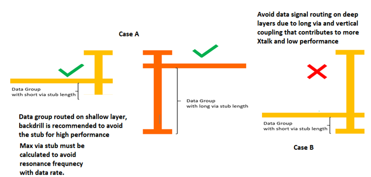
The following figure illustrates a routing example for a type-3 PCB for a DDR5 design. Intel recommends that you route Data Group signals such as DQ, DM and DQS on shallow layers as stripline, with the least Z-height via transition to avoid vertical crosstalk for high performance.
The recommended routing layers for Data Group on an 18-layer board using plated-through vias are on the top half of the PCB, such as layers 3, 5, and 7. Other signals such as CA, CTRL, and clock signals can be routed with longer Z-height via transitions on the bottom half of the PCB, such as layers 12, 14, and 16.
Minimal stub effect or back drill is recommended but not required to avoid high reflection for maximum data rate performance for a DDR5 interface. Long via stubs will affect the intersymbol interference (ISI) of the channel, but the impact of ISI is less than the impact of crosstalk for maximum performance.
You should avoid stub and use of back drill for LPDDR5 design to reach max data rate performance.

In the above figure, case A routing is suggested for DDR5 Data Group signals over case B, to support maximum data rate. If data signals are routed on deeper layers (as in case B, with long via and short stub), the impact of crosstalk is significant and causes reduced data rate and performance.
To minimize crosstalk horizontally between the signals on the same layer, PCB designers must maintain adequate signal trace-to-trace (edge to edge) space with a minimum spacing of 3 x H separation distance, where H is the dielectric thickness to the closest reference plane, as illustrated below.
