External Memory Interfaces Intel Agilex® 7 M-Series FPGA IP User Guide
A newer version of this document is available. Customers should click here to go to the newest version.
Visible to Intel only — GUID: mpc1693106509625
Ixiasoft
Visible to Intel only — GUID: mpc1693106509625
Ixiasoft
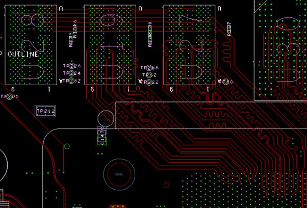
7.3.7.4. Example of a DDR5 layout on Intel FPGA Platform Board
This layout is designed on a thick PCB (120mil stackup) using micro vias and through vias with backdrill. The DDR5 Data signal routing is on upper layers to avoid vertical crosstalk and achieve high performance; the CS/CTRL signals can be routed on deeper layers.
