4.4.1. Using the Configure Menu
4.4.2. The System Info Tab
4.4.3. The GPIO Tab
4.4.4. The XCVR Tab
4.4.5. The PCIe* Tab
4.4.6. The FMCA Tab
4.4.7. The FMCB Tab
4.4.8. The DDR3 Tab
Performance Indicators
Error Control
Number of Addresses to Write and Read
4.4.9. The DDR4 Tab
4.4.10. The EEPROM Tab
4.4.11. The Power Monitor
4.4.12. The Clock Control
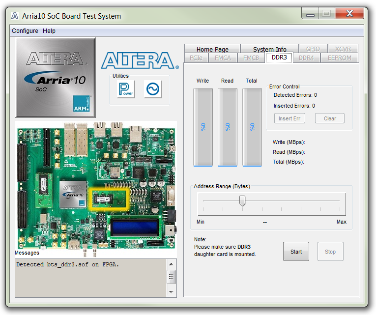
4.4.8. The DDR3 Tab
This tab allows you to read and write DDR3 memory on your board.
Figure 25. The DDR3 Tab


Performance Indicators
These controls display current transaction performance analysis information collected since you last clicked Start:
- Write, Read, and Total performance bars: Show the percentage of maximum theoretical data rate that the requested transactions are able to achieve.
- Write (MBps), Read (MBps), and Total (MBps): Show the number of bytes of data analyzed per second.
- Data bus: 72 bits (8 bits ECC) wide and the frequency is 1066 MHz double data rate. 2133 Megabits per second (Mbps) per pin. Equating to a theoretical maximum bandwidth of 136512 Mbps or 17064 Mbps.
Error Control
This control displays data errors detected during analysis and allows you to insert errors:
- Detected errors: Displays the number of data errors detected in the hardware.
- Inserted errors: Displays the number of errors inserted into the transaction stream.
- Insert Error: Inserts a one-word error into the transaction stream each time you click the button. Insert Error is only enabled during transaction performance analysis.
- Clear: Resets the Detected errors and Inserted errors counters to zeroes.
Number of Addresses to Write and Read
Determines the number of addresses to use in each iteration of reads and writes.