Intel® Quartus® Prime Pro Edition User Guide: Power Analysis and Optimization
ID
683174
Date
6/22/2022
Public
A newer version of this document is available. Customers should click here to go to the newest version.
Visible to Intel only — GUID: yro1564758686794
Ixiasoft
1.3.2.1. Using Simulation Signal Activity Data in Power Analysis
1.3.2.2. Signal Activities from RTL (Functional) Simulation, Supplemented by Vectorless Estimation
1.3.2.3. Signal Activities from Vectorless Estimation and User-Supplied Input Pin Activities
1.3.2.4. Signal Activities from User Defaults Only
1.5.1. Complete Design Simulation Power Analysis Flow
1.5.2. Modular Design Simulation Power Analysis Flow
1.5.3. Multiple Simulation Power Analysis Flow
1.5.4. Overlapping Simulation Power Analysis Flow
1.5.5. Partial Design Simulation Power Analysis Flow
1.5.6. Vectorless Estimation Power Analysis Flow
2.4.1. Clock Power Management
2.4.2. Pipelining and Retiming
2.4.3. Architectural Optimization
2.4.4. I/O Power Guidelines
2.4.5. Dynamically Controlled On-Chip Terminations (OCT)
2.4.6. Memory Optimization (M20K/MLAB)
2.4.7. DDR Memory Controller Settings
2.4.8. DSP Implementation
2.4.9. Reducing High-Speed Tile (HST) Usage
2.4.10. Unused Transceiver Channels
2.4.11. Periphery Power reduction XCVR Settings
Visible to Intel only — GUID: yro1564758686794
Ixiasoft
2.4.6.1. Implementation
| Memory Block | Depth (bits) | Programmable Width |
|---|---|---|
| MLAB | 32 | x16, x18, or x20 |
| 64 3 | x8, x9, x10 | |
| M20K | 512 | x40, x32 |
| 1K | x20, x16 | |
| 2K | x10, x8 | |
| 4K | x5, x4 | |
| 8K | x2 | |
| 16K | x1 |
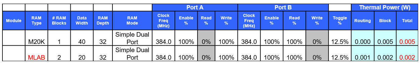
Figure 35. Power numbers from EPE
3 Supported through software emulation and consumes additional MLAB blocks.