4.2.2. Example Design Parameters for High Bandwidth Memory (HBM2E) Interface FPGA IP
The Example Design tab allows you to configure example design files for simulation and synthesis.
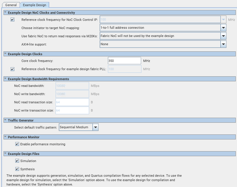
Figure 13. Example Design tab of HBM2E IP Parameters
| Display Name | Description |
|---|---|
| Reference clock frequency for example design NoC Clock Control IP | When running the design example on hardware, you can override this setting to match the NoC reference clock generated by your board. |
| Choose initiator to target NoC mapping | You can choose between two configurations of initiator to target hard memory NoC mapping for the design example:
|
| Use Fabric NoC to return read responses via M20Ks | When you enable any option other than Fabric NoC will not be used by the example design, the NoC initiator IP uses the fabric's M20K-based memories to deliver AXI read responses deep into the fabric. 512-bits of read response data are returned to your design in each AXI interface, enabling fabric frequencies above 350 MHz to saturate HBM2E pseudo-channel read bandwidth. You can enable the Fabric NoC for one of the following configurations: 512-bit wide data paths. 256-bit NoC bridge hardware has an independent clock: Configures the NoC Initiator IP with a single 512-bit wide AXI interface for both read and write data paths, in which case the NoC bridge hardware must be supplied with its own clock. The following two configurations are asymmetric modes in which the NoC Initiator IP has separate 512-bit wide read and 256-bit wide write data paths. These paths can have a common clock , but giving the wide read data paths their own clock enables a higher frequency to be used for the write interface:
|
| AXI4-Lite support | Select this option to choose a design example that includes AXI4-Lite interfaces in the fabric. The AXI4-Lite interface provides access to control and status registers. You must enable this option if you want to access the control and status registers of the HBM2E IP.
Note: You cannot enable an AXI4-Lite interface with 288-bit data mode designs.
Refer to the Use Cases topic in the HBM2E IP Design Example User Guide for more detailed information on the implementation of these options. |
| NoC read bandwidth | The anticipated read bandwidth requirement, in GBps, for each NoC initiator bridge-to-target bridge (I-T) connection. The Quartus® PrimeCompiler uses this information to analyze whether there is congestion on the hard memory NoC. This is a default value selected based on the most optimal configuration and initiator placements. This assignment is made consistently to all I-T connections in the design. The performance analysis tool may flag warnings if these requirements lead to potential congestion on the NoC. Such a design can still be fully compiled and run on hardware but may cause sub-optimal performance. These settings can be changed independently for each I-T connection in the design in the NoC assignment editor. |
| NoC write bandwidth | The anticipated write bandwidth requirement, in GBps, for each NoC initiator bridge-to-target bridge (I-T) connection. The Quartus® Prime Compiler uses this information to analyze whether there is congestion on the hard memory NoC. This is a default value selected based on the most optimal configuration and initiator placements. This assignment is made consistently to all I-T connections in the design. The performance analysis tool may flag warnings if these requirements lead to potential congestion on the NoC. Such a design can still be fully compiled and run on hardware but may cause sub-optimal performance. These settings can be changed independently for each I-T connection in the design in the NoC assignment editor. |
| NoC read transaction size | The anticipated read transaction length requirement, in B, for each NoC initiator bridge-to-target bridge (I-T) connection. The Quartus® Prime Compiler uses this information to analyze whether there is congestion on the hard memory NoC. This is a default value selected based on the most optimal configuration and initiator placements. This assignment is made consistently to all I-T connections in the design. The performance analysis tool may flag warnings if these requirements lead to potential congestion on the NoC. Such a design can still be fully compiled and run on hardware but may cause sub-optimal performance. These settings can be changed independently for each I-T connection in the design in the NoC assignment editor. |
| NoC write transaction size | The anticipated write transaction length requirement, in B, for each NoC initiator bridge-to-target bridge (I-T) connection. The Quartus® Prime Compiler uses this information to analyze whether there is congestion on the hard memory NoC. This is a default value selected based on the most optimal configuration and initiator placements. This assignment is made consistently to all I-T connections in the design. The performance analysis tool may flag warnings if these requirements lead to potential congestion on the NoC. Such a design can still be fully compiled and run on hardware but may cause sub-optimal performance. These settings can be changed independently for each I-T connection in the design in the NoC assignment editor. |
| Display Name | Description | ||||||||||||
|---|---|---|---|---|---|---|---|---|---|---|---|---|---|
| Core clock frequency | The frequency of the core clock used to drive the design example's traffic generators and the NoC initiator IP interfaces to which they connect. In cases of fabric NoC designs with 512-bit wide data paths, the NoC initiator IP have their own clock. Valid range of core clock frequencies depends on device speed grade and design details. Maximum values apply to all designs, while recommended values are based on the design example without fabric NoC.
For designs using fabric NoC, refer to the High Bandwidth Memory (HBM2E) Interface Agilex™ 7 M-Series FPGA IP Design Example User Guide. |
||||||||||||
| NoC bridge hardware frequency | Specifies the frequency of the clock that the design example uses to drive the 256-bit wide NoC bridge hardware when you configure the design example to generate NoC Initiator IP with 512-bit data paths. The following table shows the maximum operating frequency of the NoC bridge hardware for a design using Fabric NoC:
For information on different fabric NoC configurations, refer to the High Bandwidth Memory (HBM2E) Interface Agilex™ 7 M-Series FPGA IP Design Example User Guide.
Note: This parameter is available only when you choose a fabric NoC configuration of 512-bit wide data paths. 256-bit NoC bridge hardware has an independent clock.
|
||||||||||||
| Reference clock frequency for example design core clock PLL | Reference clock frequency for the PLL supplying the core clock. This parameter affects only the design example PLL. | ||||||||||||
| Read-only AXI data path frequency | Specifies the clock frequency of the NoC initiator IP read interface when you configure the design example to generate NoC Initiator IP with separately clocked asymmetric-width read and write interfaces. The following table shows the minimum operating frequency to drive the 512-bit read-only AXI data path frequency:
Note: This parameter is available only when you choose a fabric NoC configuration of 256-bit wide and 512-bit read data paths, read data path has its own clock.
|
| Display Name | Description |
|---|---|
| Select default traffic pattern | This option allows you to select the traffic pattern type and how many read and write transactions to run in the design example simulation. |
| Display Name | Description |
|---|---|
| Enable performance monitoring | Select this option to enable the performance monitor on all active HBM2E channels for measuring read and write transaction metrics. |
| Display Name | Description |
|---|---|
| Simulation | Specifies that the system generate all necessary file sets for simulation when you click Generate Example Design. If you do not enable this parameter, the system does not generate simulation file sets. Instead, the output directory contains the ed_sim.qsys file which contains details of the simulation example design for Platform Designer, and a make_sim_design.tcl file with other corresponding tcl files. You can run the make_sim_design.tcl file from a command line to generate a simulation example design. The generated example designs for various simulators reside in the /sim subdirectory. |
| Synthesis | Specifies that the system generate all necessary file sets for synthesis when you click Generate Example Design. If you do not enable this parameter, the system does not generate synthesis file sets. Instead, the output directory contains the ed_synth.qsys file which contains details of the synthesis example design for Platform Designer, and a make_qii_design.tcl file with other corresponding tcl files. You can run the make_qii_design.tcl file from a command line to generate a synthesis example design. The generated example design resides in the /qii subdirectory. |
| Display Name | Description |
|---|---|
| Simulation HDL format | Format of HDL files generated for simulating the design example. |