5.2.5. AXI4 Interface Signals
The AXI interface to the HBM2E controller follows the Amba AXI4 protocol specification. Each AXI interface serves the read and write operations for one pseudo channel, and is connected to a NoC target. Your design should issue AXI commands to the HBM2E controller(s) via one or more instances of the NoC Initiator FPGA IP. You can configure the hard memory NoC so that your design can use a single AXI interface to access any or all of the pseudo-channels. The hard memory NoC can also be configured to suit designs that use multiple AXI interfaces to initiate NoC commands to a common set of pseudo-channels.
AXI Interface Signals
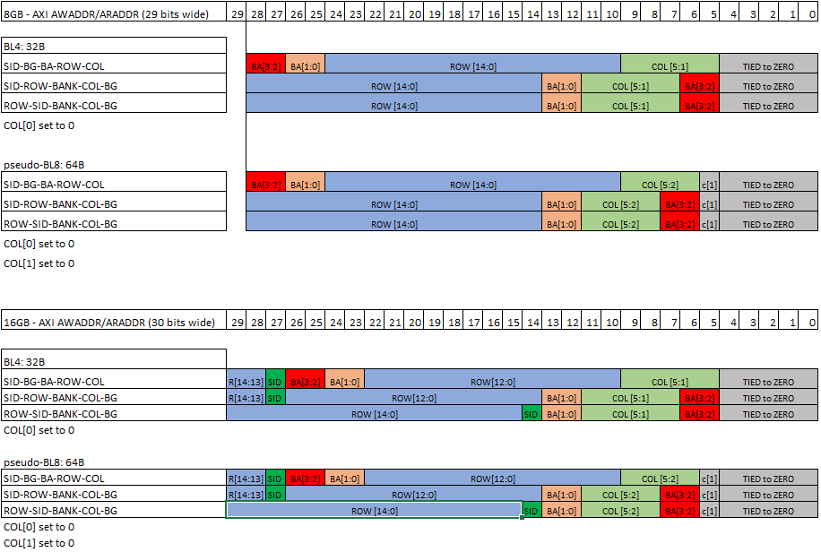
The hard memory NoC uses the upper 14 bits of AXI addresses to direct commands to the 16 HBM pseudo-channels.
Each AXI interface consists of five subchannels:
- Write Address Channel –AXI write commands, specifying the target address, transfer size, and associated information.
- Write Data Channel – AXI write data provided by the core logic corresponding to the write address.
- Write Response Channel – Response from the HBM2E controller indicating whether or not each write has been accepted.
- Read Address Channel – AXI read commands, specifying the target address, transfer size, and associated information.
- Read Data Channel – AXI read data provided from the corresponding HBM2E DRAM read address.
AXI Address Definition
The lower 30 bits of the AXI address identify a location within the targeted pseudo-channel. The HBM2E DRAM addressing consists of the following:
- 15-bit wide row address.
- 6-bit wide column address. The user logic drives column address bits COL[5:1], while the controller sets the lower order column address bit COL[0] to 0. For pBL8 transactions, the user logic must set COL[1] to 0.
- 4-bit wide bank address. Bank group corresponds to the higher order 2 bits of the bank address (BA[3:2]). HBM accesses are more efficient when the controller is able to schedule consecutive HBM2E memory device read and write commands to different bank groups.
- 1-bit wide Stack ID (SID) is available only in the 16GB configuration.
Figure 16. AXI Address Definition
HBM2E IP AXI Channel Descriptions
Within the HBM2E IP, the AXI interface signals of the HBM2E controller follow the pattern ch<x>_u<y>_<portname> where x is the channel number and y is the pseudo-channel number. For example, ch0_u1_awid refers to the write address ID of the AXI interface corresponding to channel 0 and pseudo-channel 1. These AXI interfaces are not user-accessible.
The signals in the following tables refer to the signal names corresponding to a single AXI interface: channel 0, pseudo-channel 0.
| Port Name | Width | Direction | Description | ||||||
|---|---|---|---|---|---|---|---|---|---|
| ch0_u0_awaddr | 30 | Input | Write address. The write address gives the address of the first transfer in a write burst transaction. | ||||||
| ch0_u0_awburst | 2 | Input | Burst type. The burst type and length determine how the address for each transfer within the burst is calculated.
Note: Only INCR Burst Type is supported for HBM accesses.
|
||||||
| ch0_u0_awid | 7 | Input | Write address channel command ID tag. | ||||||
| ch0_u0_awlen | 8 | Input | Burst Length. The burst length gives the exact number of transfers in an AXI burst. In BL4 mode the HBMC supports burst lengths of 1 or 2; in BL8 mode the HBMC only supports a burst length of 2. When your design uses a burst length of greater than 2, the NOC initiator hardware issues multiple AXI commands of burst length 1 or 2 to the HBMC. Note that AXI encodes a burst length of 1 as awlen = 0, and burst length 2 is encoded as awlen = 1. | ||||||
| ch0_u0_awprot | 3 | Input | Protection Type. [Reserved for future use] This signal indicates the privilege and security level of the transaction, and whether the transaction is a data access or an instruction access.
|
||||||
| ch0_u0_awqos | 4 | Input | Quality-of-service identifier for this write command. The HBM controller supports only two priority levels, distinguished by the top bit of the QoS signal.
|
||||||
| ch0_u0_awready | 1 | Output | Write Address Channel Ready. This signal indicates that the slave is ready to accept an address and associated control signals. | ||||||
| ch0_u0_awsize | 3 | Input | Burst Size. This signal indicates the number of AXI byte lanes containing valid data in each transfer of the burst.
Note: The HBM controller supports only 256/288-bits (32 bytes) access, burst size must be driven to 3’b101.
|
||||||
| ch0_u0_awuser | 14 | Input | Intel-defined signals: auto-precharge is signaled on awuser[0]. awuser[13:1] must be driven to 13'b0 at the HBM controller interface. | ||||||
| ch0_u0_awvalid | 1 | Input | Write Address Channel Valid. This signal indicates that valid write address and control information are available. | ||||||
| ch0_u0_awlock | 1 | Input | Lock Type [Reserved for future use]. |
| Port Name | Width | Direction | Description |
|---|---|---|---|
| ch0_u0_wdata | 256 | Input | Write Data. |
| ch0_u0_wlast | 1 | Input | Write Last. This signal indicates the last transfer in a write burst. |
| ch0_u0_wready | 1 | Output | Write Channel Ready. This signal indicates that the slave (HBM controller) can accept the write data. |
| ch0_u0_wstrb | 32 | Input | Write Strobes (Byte Enables). This signal indicates which byte lanes (for ch0_u0_wdata) hold valid data. There is one write strobe bit for each eight bits of the write data bus. |
| ch0_u0_wuser | 32 | Input | Intel-defined signal: when the pseudo-channel's Data Mode is set to 288-bit, the ECC bits of the HBM device receive their value from wuser. |
| ch0_u0_wvalid | 1 | Input | Write Channel Valid. This signal indicates that valid write data and strobes are available. |
| Port Name | Width | Direction | Description | ||||||
|---|---|---|---|---|---|---|---|---|---|
| ch0_u0_bid | 7 | Output | Response ID Tag. This signal is the ID tag of the write response, and matches the ID tag of the command for which this is the response. | ||||||
| ch0_u0_bready | 1 | Input | Write Response Channel Ready. This signal indicates that the master can accept a write response. | ||||||
| ch0_u0_bresp | 2 | Output | Write Response. This signal indicates the result of the write command.
|
||||||
| ch0_u0_bvalid | 1 | Output | Write Response Channel Valid. This signal indicates that a valid write response is available. |
| Port Name | Width | Direction | Description | ||||||
|---|---|---|---|---|---|---|---|---|---|
| ch0_u0_araddr | 30 | Input | Read Address. The read address gives the address of the first transfer in a read burst transaction. | ||||||
| ch0_u0_arburst | 2 | Input | Burst type. The burst type and length determine how the address for each transfer within the burst is calculated.
Note: Only INCR Burst Type is supported by the HBM controller.
|
||||||
| ch0_u0_arid | 7 | Input | Read address channel command ID tag. | ||||||
| ch0_u0_arlen | 8 | Input | Burst Length. The burst length gives the exact number of transfers in an AXI burst. In BL4 mode the HBMC supports burst lengths of 1 or 2; in pseudo-BL8 mode the HBMC only supports a burst length of 2. When your design uses a burst length of greater than 2, the NOC initiator hardware issues multiple AXI commands of burst length 1 or 2 to the HBMC. Note that AXI encodes a burst length of 1 as arlen = 0, and burst length 2 is encoded as arlen = 1. | ||||||
| ch0_u0_arprot | 3 | Input | Protection Type. [Reserved for future use.] This signal indicates the privilege and security level of the transaction, and whether the transaction is a data access or an instruction access.
Because secure transactions are currently not supported by the HBM controller, this value must be driven to 3’b010. |
||||||
| ch0_u0_arqos | 4 | Input | Quality-of-service identifier for this read command. The HBM controller supports only two priority levels, distinguished by the top bit of the QoS signal.
|
||||||
| ch0_u0_arready | 1 | Output | Read Address Ready. This signal indicates that the slave is ready to accept an address and associated control signals. | ||||||
| ch0_u0_arsize | 3 | Input | Burst Size. This signal indicates the number of AXI byte lanes containing valid data in each transfer in the burst. NOTE: The HBM controller supports only 256/288-bits (32 bytes) access, burst size must be driven to 3’b101. | ||||||
| ch0_u0_aruser | 14 | Input | Intel-defined signals: auto-precharge is signaled on aruser[0]. aruser[13:1] must be driven to 13'b0 at the HBM controller interface. | ||||||
| ch0_u0_arvalid | 1 | Input | Read Address Valid. This signal indicates that valid read address and control information are available. | ||||||
| ch0_u0_arlock | 1 | Input | Lock Type [Reserved for future use]. |
| Port Name | Width | Direction | Description | ||||||
|---|---|---|---|---|---|---|---|---|---|
| ch0_u0_rdata | 256 | Output | Read Data. | ||||||
| ch0_u0_rid | 7 | Output | Read Response ID Tag. This signal is the ID tag for the read response, and matches the ID tag of the command for which this is the response. | ||||||
| ch0_u0_rlast | 1 | Output | Read Last. This signal indicates the last transfer in a read burst. | ||||||
| ch0_u0_rready | 1 | Input | Read Response Channel Ready. This signal indicates that the master can accept the read data and response information. | ||||||
| ch0_u0_rresp | 2 | Output | Read Response. This signal indicates the result of the read command.
|
||||||
| ch0_u0_ruser | 32 | Output | Intel-defined signal: when the pseudo-channel's Data Mode is set to 288-bit, this signal receives its value from the ECC bits of the HBM device. | ||||||
| ch0_u0_rvalid | 1 | Output | Read Valid. This signal indicates that a valid read response is available. |