Intel® FPGA SDK for OpenCL™ Pro Edition: Best Practices Guide
A newer version of this document is available. Customers should click here to go to the newest version.
3.2. Global Memory Interconnect
Unlike a GPU, an FPGA can build any custom LSU that is best suited for the memory access pattern that the compiler infers for your application. As a result, your ability to write OpenCL code that selects the ideal LSU types for your application might help improve the performance of your design significantly.
When reviewing the HTML area report of your design, the values in the Global interconnect entry at the system level represents the size of the global memory interconnect.

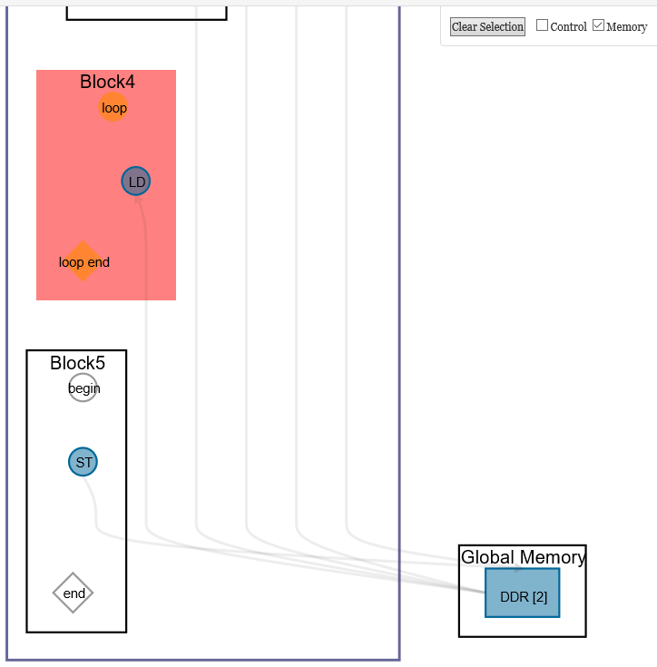
In the HTML report, the system view of the System Viewer depicts global memory interconnects as loads (LD), stores (ST), and connections (gray lines).

The Intel® FPGA SDK for OpenCL Offline Compiler selects the appropriate type of LSU for your OpenCL system based on the memory access pattern of your design. Example LSU types include contiguous access (or consecutive access) and burst-interleaved access. Contiguous Memory Access and Global Memory Partitions illustrate the difference in access patterns between contiguous and burst-interleaved memory accesses, respectively.