Visible to Intel only — GUID: epa1614373378122
Ixiasoft
1.1. Hardware and Software Requirements
1.2. Generating the Design Example
1.3. Directory Structure
1.4. Simulating the Design Example
1.5. Compiling the Compilation-Only Project
1.6. Compiling and Configuring the Design Example in Hardware
1.7. Testing the Hardware Design Example
1.8. Transceiver Toolkit
Visible to Intel only — GUID: epa1614373378122
Ixiasoft
1.2. Generating the Design Example
Follow these steps to generate the F-Tile CPRI PHY IP hardware design example and testbench.
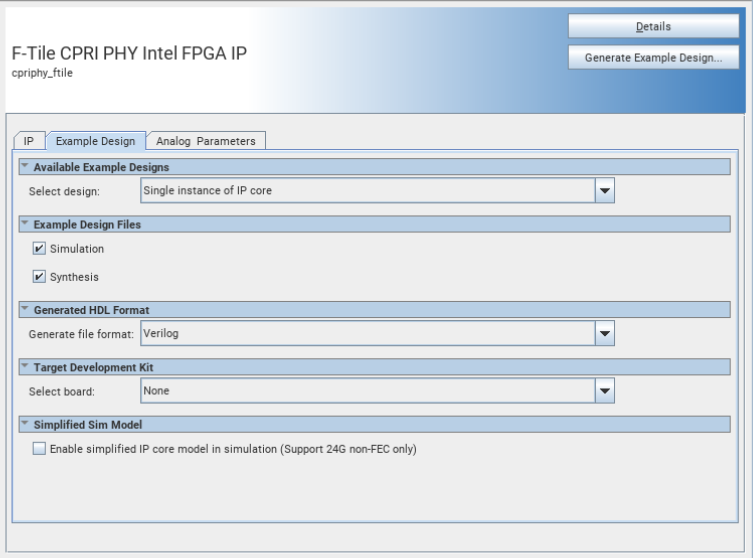
Figure 2. Example Design Tab in IP Parameter Editor
- Create an Quartus® Prime Pro Edition project:
- In the Quartus® Prime Pro Edition software, click File > New Project Wizard to create a new project, or File > Open Project to open an existing project. The wizard prompts you to specify a device.
- Specify the device family Agilex™ 7 (I-series) and select a device that meets all of these requirements:
- Transceiver tile: F-tile
- Transceiver speed grade: -1 or -2
- Core speed grade: -1 or -2 or -3
- Click Finish.
- In the IP Catalog, locate and select F-Tile CPRI PHY Intel® FPGA IP. The New IP Variation dialog box appears.
- Specify a top-level name for your custom IP variation. The parameter editor saves the IP variation settings in a file named <your_ip> .ip.
- Click OK. The parameter editor appears.
- On the IP tab, specify the parameters for your IP core variation.
- On the Example Design tab:
- Under Example Design Files, select the Simulation option to generate the testbench and the compilation-only project. Select the Synthesis option to generate the hardware design example. You must select at least one of the Simulation and Synthesis options to generate the design example.
- Under Generated HDL Format, select Verilog HDL or VHDL. If you select VHDL, you must simulate the testbench with a mixed-language simulator. The device under test in the ex_<datarate> directory is a VHDL model, but the main testbench file is a SystemVerilog file.
- Under Target Development Kit, select your board.
- Turn on Simplified testbench for a testbench that allows you to emulate the simulation flow of the standard testbench with shorter simulation time.
This simplified testbench does not provide deterministic latency or the serial functionality, and supports only 24G non-FEC speed rate without 8B10B reconfiguration option.
- On the Analog Parameters tab, select the correct parameters for your design example. Refer to Analog Parameters Tab
- Click the Generate Example Design button. The Select Example Design Directory dialog box appears.
- To modify the design example directory path or name from the defaults (cpriphy_ftile_0_example_design), browse to the new path and type the new design example directory name (<design_example_dir>).