Visible to Intel only — GUID: xjs1518024683660
Ixiasoft
Visible to Intel only — GUID: xjs1518024683660
Ixiasoft
1.1. FPGA Overview

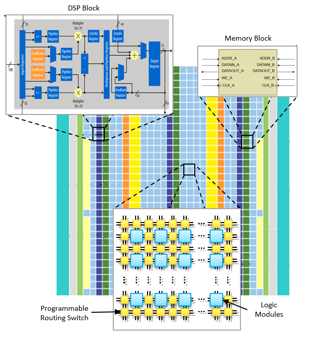
With FPGAs, low-level operations like bit masking, shifting, and addition are all configurable. Also, you can assemble these operations in any order. To implement computation pipelines, FPGAs integrate combinations of lookup tables (LUTs), registers, on-chip memories, and arithmetic hardware (for example, digital signal processor (DSP) blocks) through a network of reconfigurable connections. As a result, FPGAs achieve a high level of programmability. LUTs are responsible for implementing various logic functions. For example, reprogramming a LUT can change an operation from a bit-wise AND logic function to a bit-wise XOR logic function.
The key benefit of using FPGAs for algorithm acceleration is that they support wide, heterogeneous and unique pipeline implementations. This characteristic is in contrast to many different types of processing units such as symmetric multiprocessors, DSPs, and graphics processing units (GPUs). In these types of devices, parallelism is achieved by replicating the same generic computation hardware multiple times. In FPGAs, however, you can achieve parallelism by duplicating only the logic that your algorithm exercises.
A processor implements an instruction set that limits the amount of work it can perform each clock cycle. For example, most processors do not have a dedicated instruction that can execute the following C code:
E = (((A + B) ^ C) & D) >> 2;
Without a dedicated instruction for this C code example, a CPU, DSP, or GPU must execute multiple instructions to perform the operation. In contrast, you may think of an FPGA as a hardware platform that can implement any instruction set that your software algorithm requires. You can configure an FPGA to perform a sequence of operations that implements the code example above in a single clock cycle. An FPGA implementation connects specialized addition hardware with a LUT that performs the bit-wise XOR and AND operations. The device then leverages its programmable connections to perform a right shift by two bits without consuming any hardware resources. The result of this operation then becomes a part of subsequent operations to form complex pipelines.