Visible to Intel only — GUID: lro1429463779662
Ixiasoft
2.1. Starting the Flash Programmer GUI
2.2. Specifying your Flash Programmer Settings
2.3. Working with Flash Programmer Settings Files
2.4. Setting the Hardware Connection
2.5. Checking System ID and System Timestamp
2.6. Generating Flash Files and Programming Flash Memory
2.7. Document Revision History for Using the Flash Programmer GUI
B.1. Overview
B.2. Start Button Grayed Out in the Flash Programmer GUI
B.3. 'No Nios® II Processors Available' Error
B.4. 'No CFI Table Found' Error
B.5. 'No EPCS Registers Found' Error
B.6. 'System Does Not Have Any Flash Memory' Error
B.7. 'Reading System ID at Address 0x<address>: FAIL' Error
B.8. 'Base Address Not Aligned on Size of Device' Error
B.9. Document Revision History for Troubleshooting
Visible to Intel only — GUID: lro1429463779662
Ixiasoft
1.3.1. Flash Programmer Target Design
To use the Nios® II Flash Programmer, you must have a valid flash programmer target design downloaded to your board. A valid target design contains a Platform Designer system with at least the Platform Designer components shown in the "Minimum Component Set for the Flash Programmer Target Design" table.
The minimum component set provides facilities for the target design to communicate with the host and to write to flash memory. The minimum component set depends on the type of flash memory you intend to program. "Minimum Component Set for the Flash Programmer Target Design" lists the minimum component set for programming each kind of flash memory.
| Component | Flash Memory to Program | |||
|---|---|---|---|---|
| CFI | EPCS/EPCQx1 | EPCQ | On-Chip Flash ( Intel® MAX® 10) | |
| Nios® II processor, with JTAG debug module level1 or greater | Required | Required | Required | Required |
| System ID peripheral | Recommended | Recommended1 | Recommended1 | Optional |
| Generic Tri-State Controller | Required | |||
| Tristate Conduit Bridge | Required3 | |||
| Legacy EPCS/EPCQx1 Flash Controller | Required | |||
| Intel FPGA Generic Quad SPI Controller | Required 4 | |||
| Intel FPGA Generic Quad SPI Controller II | Required4 | |||
| Intel FPGA Serial Flash Controller | Required4 | |||
| Intel FPGA Serial Flash Controller II | Required4 | |||
| Intel On-Chip Flash | Required | |||
Figure 2. Example Target Design Containing the Minimum Component SetThis is an example of a Platform Designer system with the minimum component set for a system composed of an EPCS serial configuration device. The system also includes other components which relate to the purpose of the system, not to the flash programmer.
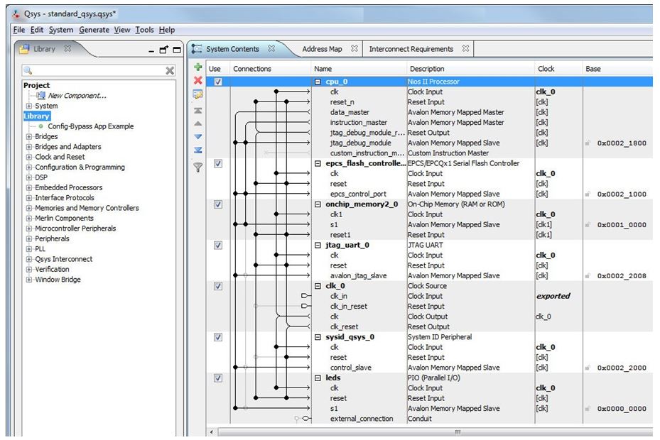
Note: The data master and instruction master of the Nios® II Processor must be connected to the same address space as the On-Chip memory.
Hardware example designs capable of programming the flash memory are provided with development boards. If you are developing for a custom board, consider using one of these example designs as a starting point for your flash programmer target design.
1 If present, a System ID Peripheral component allows the Nios II Flash Programmer to validate the target design before programming the flash memory.
2 A Nios® II system can interface with more than one CFI flash memory device. The system must contain one Flash Memory (Common Flash Interface) component for each flash memory device on the board.
3 Tri-state Conduit Bridge is needed to drive the CFI flash memory signals.
4 Only one of these components is required. Use these controllers to communicate with an EPCQ device in ASx4 mode.