Visible to Intel only — GUID: loy1698956250224
Ixiasoft
2.1. Parameterizing the HPS Component
2.2. HPS-FPGA Interfaces
2.3. SDRAM
2.4. HPS Clocks, Reset, Power
2.5. I/O Delays
2.6. Pin Mux and Peripherals
2.7. Generating and Compiling the HPS Component
2.8. Using the Address Span Extender Component
2.9. Configuring the Agilex™ 5 Hard Processor System Component Revision History
2.2.1.1. Enable MPU Standby and Event Signals
2.2.1.2. Enable General Purpose Signals
2.2.1.3. Enable Debug APB* Interface
2.2.1.4. Enable System Trace Macrocell (STM) Hardware Events
2.2.1.5. Enable SWJ-DP JTAG Interface
2.2.1.6. Enable FPGA Cross Trigger Interface
2.2.1.7. Enable AMBA* Trace Bus (ATB)
3.1. Simulation Flows
3.2. Running the Simulation of the Design Examples
3.3. Clock and Reset Interface
3.4. FPGA-to-HPS AXI* Subordinate Interface
3.5. FPGA-to-SDRAM AXI* Subordinate Interface
3.6. HPS-to-FPGA AXI* Initiator Interface
3.7. Lightweight HPS-to-FPGA AXI* Initiator Interface
3.8. Simulating the Agilex™ 5 HPS Component Revision History
Visible to Intel only — GUID: loy1698956250224
Ixiasoft
3.2.2. Lightweight HPS-to-FPGA (LWH2F)
This example instantiates an HPS initiator along with an On-Chip Memory subordinate component in Platform Designer. The testbench uses the Mentor Graphics* AXI* 4 Initiator BFM to model the HPS AXI* Bridge communication with the FPGA core logic.
- AXI* Initiator— Mentor Graphics* AXI* 4 Initiator BFM
- AXI* Subordinate—On-Chip Memory
Setup:
- Download the Example Design using this link: Hard Processor System Component Reference Manual: Agilex™ 5 SoCs - Lightweight HPS-to-FPGA Design Example.
- Uncompress the Example Design, the top directory is “agilex5_hps_lwh2f_simulation/”.
- In the top directory, verify the following items:
| File or directory |
Description |
|---|---|
| agilex5_hps_lwh2f_simulation.qsys | The top-level Platform Designer system file, which instantiates the HPS simulation model, a clock source, and a reset source. |
| ip/agilex5_hps_lwh2f_simulation | The On-Chip Memory files |
| master_test_program.sv | The Master Test Program file which initiates the transactions from HPS to FPGA fabric. |
| agilex5_hps_lwh2f_simulation_tb.v | The testbench top file which contains the Platform Designer system and the Master Test Program instantiated along with clock and reset BFMs. |
| agilex5_hps_lwh2f_simulation_tb/ | The directory contains the generated simulation scripts. |
| run.do | The QuestaSim* simulation script which uses the generated script from Platform Designer and run the simulation. |
| wave.do | The waveform file |
Simulation Mechanism:
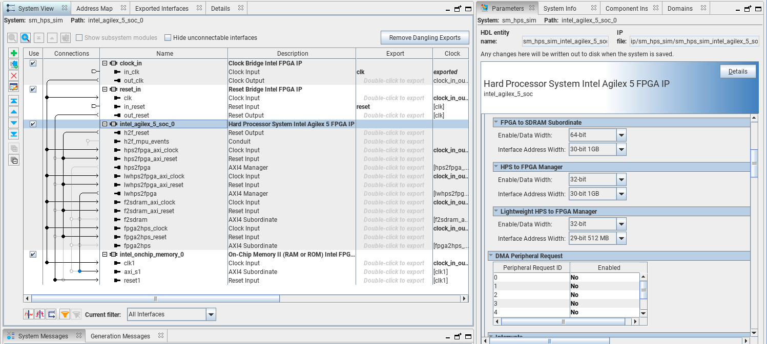
- The Platform Designer system consists of a HPS simulation model, a Clock Bridge, a Reset Bridge, and an On-Chip Memory.
Figure 54. Platform Designer System View
 Note: When prompted to upgrade the HPS IP and On-Chip RAM IP in Quartus® Prime Pro Edition version 24.3 and newer, you must manually remove the existing IPs in the design and re-instantiate them. Refer to Generating the HPS Simulation Model in Platform Designer for instructions on re-generating the simulation models.
 - The test program sends commands from the HPS BFM model using the lwh2f AXI* Bridge interface to the On-Chip memory.
- The test program performs a directed test to initiate four writes followed by four reads, and then followed by two write data bursts and two read data bursts.
- Finally, the test program verifies that the data read from the AXI* Subordinate memory matches the data written.