Visible to Intel only — GUID: pwc1658414800207
Ixiasoft
1. About the High Bandwidth Memory (HBM2E) Interface FPGA IP Design Example User Guide
2. High Bandwidth Memory (HBM2E) Interface FPGA IP Design Example Quick Start Guide
3. High Bandwidth Memory (HBM2E) Interface FPGA IP Design Example Description
4. Document Revision History for High Bandwidth Memory (HBM2E) Interface FPGA IP Design Example User Guide
2.1. Creating an Quartus® Prime Project for Your HBM2E System
2.2. Configuring the High Bandwidth Memory (HBM2E) Interface FPGA IP
2.3. Generating the High Bandwidth Memory (HBM2E) Interface FPGA IP Design Example for Synthesis and Simulation
2.4. Compiling and Programming the Agilex™ 7 M-Series High Bandwidth Memory (HBM2E) Interface FPGA IP Design Example
2.5. Using the HBM2E Design Example with the Test Engine IP
2.6. Enabling and Using the HBM2E Design Example with the Performance Monitor
2.7. Using the AXI4-Lite-enabled HBM2E Design Example in Hardware and Simulation
2.8. Simulating the High Bandwidth Memory (HBM2E) Interface FPGA IP
2.8.1. High Bandwidth Memory (HBM2E) Interface FPGA IP Example Design For Simulation
2.8.2. Simulating High Bandwidth Memory (HBM2E) Interface FPGA IP with Synopsys VCS*
2.8.3. Simulating the HBM2E FPGA IP with ModelSim SE
2.8.4. Simulating the HBM2E FPGA IP with Cadence* Xcelium Parallel Simulator
2.8.5. Simulating High Bandwidth Memory (HBM2E) Interface IP Instantiated in Your Project
Visible to Intel only — GUID: pwc1658414800207
Ixiasoft
2.3. Generating the High Bandwidth Memory (HBM2E) Interface FPGA IP Design Example for Synthesis and Simulation
To generate the design example for synthesis and simulation, follow the steps below.
Note: Before generating the design example, you must first configure the IP parameters on the General tab of the HBM2E IP parameter editor, according to your usage model. For information on the parameters of the General tab, refer to the Creating and Parameterizing the High Bandwidth Memory (HBM2E) Interface FPGA IP section in the High Bandwidth Memory (HBM2E) Interface Agilex™ 7 M-Series FPGA IP User Guide.
- On the Example Design tab, specify the desired initiator-to-target connectivity by selecting an option from the Choose initiator to target NoC mapping dropdown.
- For fabric NoC usage, select the desired option from the Use fabric NoC to return read responses via M20Ks dropdown menu.
(Refer to Fabric NoC for details on these options.)
- Select the appropriate option from the AXI4-Lite Support parameter dropdown to enable the AXI4-Lite interface in your design example.
(Refer to AXI4-Lite Support for details on these options.)
- The Example Design tab shows the read and write bandwidth for a single initiator-to-target connection, based on the core clock frequency at which the design example is running. The following example shows how the read/write bandwidth is calculated in your design:
For a design with a one-to-one initiator-to-target mapping and a core clock of 350 MHz, the following calculation applies:
Read/write bandwidth (n GBps)=
((Initiator port width (32B)  x core clock frequency (MHz ) / 1000) * EFFICIENCY FACTOR
= (32B*660)/1000*0.9
= 19GBps
Note that the actual bandwidth may vary due to congestion on the hard memory NoC. The design example displays the default optimal anticipated bandwidth for the ideal initiator placements only. - In the Example Design Clocks group box, specify a Core clock frequency for your design. Ensure that the Reference clock frequency for example design core clock PLL value matches the PLL reference clock frequency that you intend to use. (If you specified a fabric NoC option with an independent read interface or NoC bridge clock, specify the frequency of that clock in the Example Design Clocks group box.)
- In the Example Design Files group box, select Synthesis to generate a synthesizable design example, and Simulation to produce a simulation design example. You may select either or both.
Note: The design example generation for simulation does not create a separate registration function (.inc) file because the registration statements are embedded in the ed_sim.v file that is created following successful design example generation.
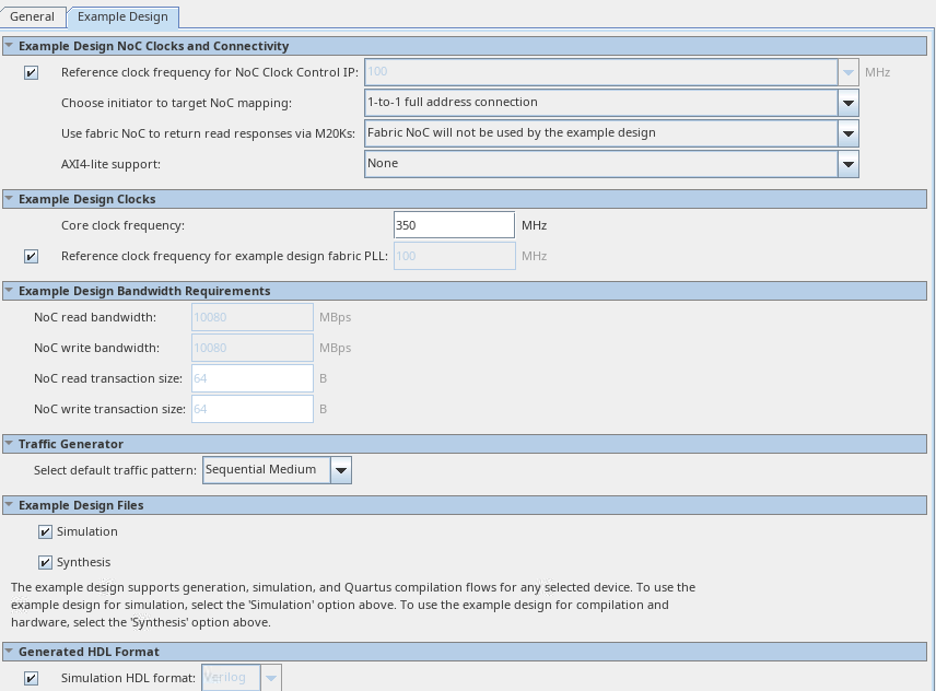 Note: The system enables both the Simulation and Synthesis checkboxes by default.
 - Click File > Save. The system creates and saves the current settings in the user IP variation file (<user instance name>.ip), within the <user project directory> that you specified.
- Click Generate Example Design at the top-right corner of the window.
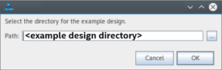
- Specify a directory for the generated design example (<design example directory>) and click OK. The system creates the design example file sets within the specified directory.
- To exit the IP Parameter Editor Pro window, click File > Exit. The system prompts, Recent changes have not been generated. Generate now? Click No to continue with the next flow.
- To open the synthesis design example, click File > Open Project, and navigate to the <project_directory>/<example_design_directory>/qii/ed_synth.qpf and click Open.
Figure 2. Generated Synthesizable Design Example File Structure
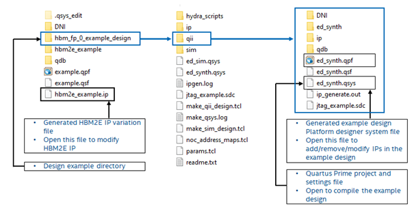
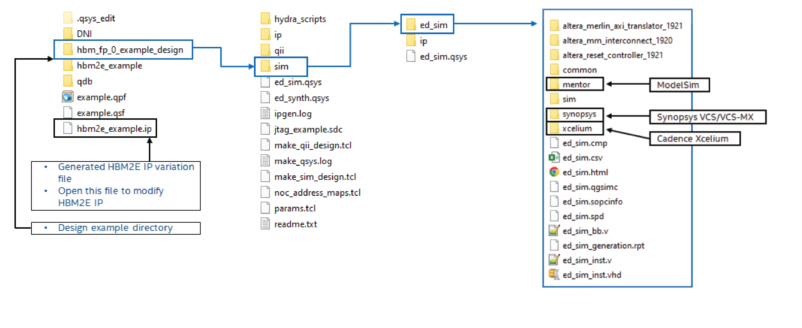
Figure 3. Generated Simulation Design Example File Structure