Visible to Intel only — GUID: jer1638456131887
Ixiasoft
1. About This Document
2. About the Nios® V Embedded Processor
3. Nios® V Processor Hardware System Design with Intel® Quartus® Prime Pro Edition and Platform Designer
4. Nios® V Processor Software System Design
5. Nios® V Processor Configuration and Booting Solutions
6. Nios® V Processor - Using the MicroC/TCP-IP Stack
7. Nios® V Processor Debugging, Verifying, and Simulating
8. Nios® V Embedded Processor Design Handbook Archives
9. Document Revision History for the Nios® V Embedded Processor Design Handbook
5.1. Introduction
5.2. Linking Applications
5.3. Nios® V Processor Booting Methods
5.4. Introduction to Nios® V Processor Booting Methods
5.5. Nios® V Processor Booting from Configuration QSPI Flash
5.6. Nios V Processor Booting from On-Chip Memory (OCRAM)
5.7. Summary of Nios V Processor Vector Configuration and BSP Settings
7.4.1. Prerequisites
7.4.2. Setting Up and Generating Your Simulation Environment in Platform Designer
7.4.3. Creating Nios V Processor Software
7.4.4. Generating Memory Initialization File
7.4.5. Generating System Simulation Files
7.4.6. Running Simulation in the QuestaSim Simulator Using Command Line
Visible to Intel only — GUID: jer1638456131887
Ixiasoft
5.5.1.1.3. Programming Files Generation
JTAG Indirect Configuration File (.jic) Generation
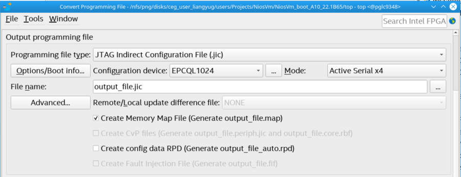
- In the Intel® Quartus® Prime Pro Edition software, go to File > Convert Programming Files.
- For Programming file type, select JTAG Indirect Configuration File (.jic)
- For Mode select Active Serial x4.
Figure 29. Convert Programming File Window

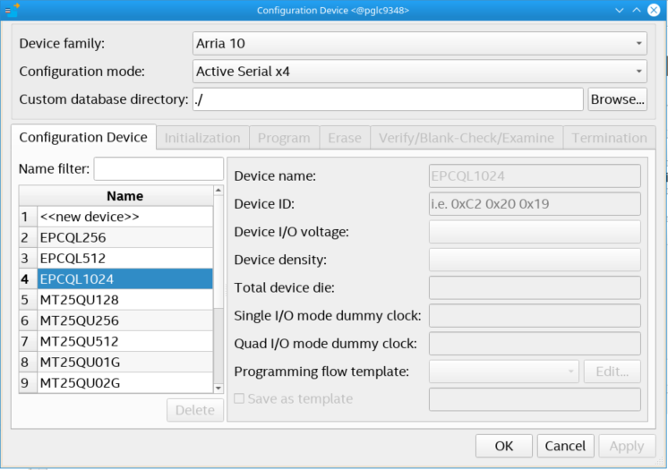
- Click “…” to enter the Configuration Device tab and select the available options. The Configuration Device allows for choosing a specific supported device or alternatively an unsupported device.
Figure 30. Configuration Device Window

- If you are using a supported device, make your selection, and click OK. Else, proceed with the following steps:
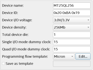
- Select <<new device>>.
- Enter the information about Device name, Device ID, Device I/O voltage, Device density, Total device die, Dummy clock (Single I/O or Quad I/O mode) and Programming flow template.
- Click Apply.
Note: The Programming flow template helps you define a template for flash operation in Initialization, Program, Erase, Verify/Blank-Check/Examine and Termination. If the device is not available for selection, refer to Modifying Programming Flows in Generic Flash Programmer User Guide to modify the programming flow. For details about memory parameters like dummy clock cycles, please contact the related vendor.

- Under the Input files to convert tab,
- Choose the Flash Loader for the FPGA used by selecting Flash Loader and click Add Device.
- Add the .sof file to the SOF Data by selecting SOF Data and click Add File.
- Click Add Hex Data to add Nios® V application (.hex) file. Select the Absolute addressing and Big-endian button. Browse to the .hex file location. Click OK.
- Click Generate to generate the JIC file.
Figure 31. Input files to convert tab

