Performance and Resource Utilization for the IO Module Design Example for OPC UA
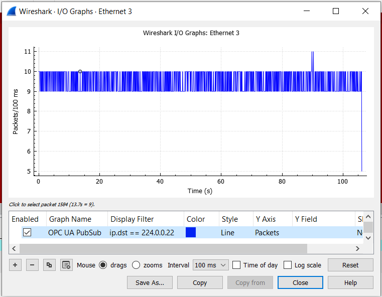
Intel used the Wireshark packet inspection tool on a client PC to monitor the incoming packets (filtered to the IP address of the IO module). The tool outputs the average packets per second, which is equivalent to the packet frequency. Intel compared different variations of frame contents: one with an empty dataset, one with 4 fields in the dataset that don’t update (static), and one where the four dataset values update on every publishing cycle (dynamic).
The data in the figure suggests that changing the system clock frequency increases the publishing performance. However ,this effect is less significant as the packet size gets larger.
The time difference between static fields and dynamic fields is 3.39 ms (40 packets/s @ 100 MHz) and 3.72 ms (58.9 packets/s @ 125 MHz), which you can attribute to the time it takes to read the IO and update the OPC UA datasets.
The time difference between 4 (static) fields and 0 fields is 2.60 ms (68.3 packets/s @ 100 MHz) and 2.55 ms (108.2 packets/s @ 125 MHz), which is a result of the difference in size of the dataset. A larger dataset takes more time to read from memory and write to the published frames.

This tool also shows that each packet (or frame) has a size of 63 bytes, which is dependent on the complexity of the informational model in the publisher.

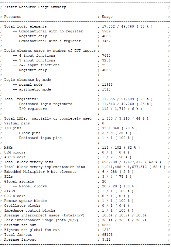
Intel optimizes the FPGA resource utilization for timing constraints, port sizes, and memory allocation. The design uses 35% of the FPGA logic, 62% of the on-chip M9K memory blocks, and 20% of the potential IO pins.
