Visible to Intel only — GUID: lbl1443214029115
Ixiasoft
1. Datasheet
2. Getting Started with the SR-IOV Design Example
3. Parameter Settings
4. Physical Layout
5. Interfaces and Signal Descriptions
6. Registers
7. Reset and Clocks
8. Programming and Testing SR-IOV Bridge MSI Interrupts
9. Error Handling
10. IP Core Architecture
11. Design Implementation
12. Debugging
13. Document Revision History
A. Transaction Layer Packet (TLP) Header Formats
B. Arria® 10 Avalon-ST with SR-IOV Interface for PCIe Solutions User Guide Archive
3.1. Parameters
3.2. Arria® 10 Avalon-ST Settings
3.3. Arria® 10 SR-IOV System Settings
3.4. Base Address Register (BAR) Settings
3.5. SR-IOV Device Identification Registers
3.6. Arria® 10 Interrupt Capabilities
3.7. Physical Function TLP Processing Hints (TPH)
3.8. Address Translation Services (ATS)
3.9. PCI Express and PCI Capabilities Parameters
3.10. PHY Characteristics
3.11. Example Designs
5.1. Avalon-ST TX Interface
5.2. Component-Specific Avalon-ST Interface Signals
5.3. Avalon-ST RX Interface
5.4. BAR Hit Signals
5.5. Configuration Status Interface
5.6. Clock Signals
5.7. Function-Level Reset (FLR) Interface
5.8. SR-IOV Interrupt Interface
5.9. Configuration Extension Bus (CEB) Interface
5.10. Implementing MSI-X Interrupts
5.11. Control Shadow Interface
5.12. Local Management Interface (LMI) Signals
5.13. Reset, Status, and Link Training Signals
5.14. Hard IP Reconfiguration Interface
5.15. Serial Data Signals
5.16. Test Signals
5.17. PIPE Interface Signals
5.18. Arria® 10 Development Kit Conduit Interface
6.1. Addresses for Physical and Virtual Functions
6.2. Correspondence between Configuration Space Registers and the PCIe Specification
6.3. PCI and PCI Express Configuration Space Registers
6.4. MSI Registers
6.5. MSI-X Capability Structure
6.6. Power Management Capability Structure
6.7. PCI Express Capability Structure
6.8. Advanced Error Reporting (AER) Enhanced Capability Header Register
6.9. Uncorrectable Error Status Register
6.10. Uncorrectable Error Mask Register
6.11. Uncorrectable Error Severity Register
6.12. Correctable Error Status Register
6.13. Correctable Error Mask Register
6.14. Advanced Error Capabilities and Control Register
6.15. Header Log Registers 0-3
6.16. SR-IOV Virtualization Extended Capabilities Registers
6.17. Virtual Function Registers
6.16.1. SR-IOV Virtualization Extended Capabilities Registers Address Map
6.16.2. ARI Enhanced Capability Header
6.16.3. SR-IOV Enhanced Capability Registers
6.16.4. Initial VFs and Total VFs Registers
6.16.5. VF Device ID Register
6.16.6. Page Size Registers
6.16.7. VF Base Address Registers (BARs) 0-5
6.16.8. Secondary PCI Express Extended Capability Header
6.16.9. Lane Status Registers
6.16.10. Transaction Processing Hints (TPH) Requester Enhanced Capability Header
12.1.1. Changing Between Serial and PIPE Simulation
12.1.2. Using the PIPE Interface for Gen1 and Gen2 Variants
12.1.3. Viewing the Important PIPE Interface Signals
12.1.4. Disabling the Scrambler for Gen1 and Gen2 Simulations
12.1.5. Disabling 8B/10B Encoding and Decoding for Gen1 and Gen2 Simulations
Visible to Intel only — GUID: lbl1443214029115
Ixiasoft
2.2. Design Components for the SR-IOV Design Example
Figure 4. Platform Designer Testbench for Arria® 10 Gen1 x8 128-bit SR-IOV Design Example
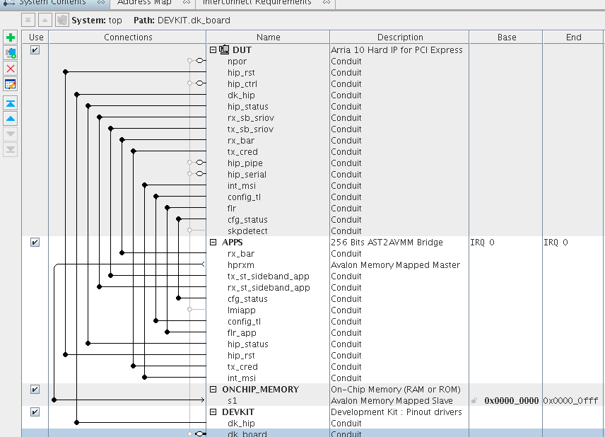
Figure 5. Platform Designer Schematic for TopThis image of the Arria® 10 PCI Express DMA Design Example shows only the Avalon-ST, clock, and reset interfaces.


The testbench includes a PCIe Root Port BFM and a PCIe Gen3 x8 Endpoint implemented in hard logic. The SR-IOV bridge, implemented in soft logic, drives memory writes and reads to the four VFs. The simulation includes the following stages:
- Link Training
- Configuration
- Memory writes to each VF
- Memory reads and compares to the expected data