Visible to Intel only — GUID: was1702425092796
Ixiasoft
1. Stratix® 10 Embedded Memory Overview
2. Stratix® 10 Embedded Memory Architecture and Features
3. Stratix® 10 Embedded Memory Design Considerations
4. Stratix® 10 Embedded Memory IP References
5. Intel Stratix 10 Embedded Memory Design Example
6. Stratix® 10 Embedded Memory User Guide Archives
7. Document Revision History for the Stratix® 10 Embedded Memory User Guide
2.1. Byte Enable in Stratix® 10 Embedded Memory Blocks
2.2. Address Clock Enable Support
2.3. Asynchronous Clear and Synchronous Clear
2.4. Memory Blocks Error Correction Code (ECC) Support
2.5. Force-to-Zero
2.6. Coherent Read Memory
2.7. Freeze Logic
2.8. True Dual Port Dual Clock Emulator
2.9. 'X' Propagation Support in Simulation
2.10. Stratix® 10 Supported Embedded Memory IPs
2.11. Stratix® 10 Embedded Memory Clocking Modes
2.12. Stratix® 10 Embedded Memory Configurations
2.13. Initial Value of Read and Write Address Registers
3.1. Consider the Memory Block Selection
3.2. Consider the Concurrent Read Behavior
3.3. Read-During-Write (RDW)
3.4. Consider Power-Up State and Memory Initialization
3.5. Reduce Power Consumption
3.6. Avoid Providing Non-Deterministic Input
3.7. Avoid Changing Clock Signals and Other Control Signals Simultaneously
3.8. Including the Reset Release Intel® FPGA IP in Your Design
3.9. Resource and Timing Optimization Feature in MLAB Blocks
3.10. Consider the Memory Depth Setting
3.11. Consider Registering the Memory Output
4.1.1. Release Information for RAM and ROM Intel® FPGA IPs
4.1.2. RAM: 1-PORT Intel® FPGA IP Parameters
4.1.3. RAM: 2-PORT Intel® FPGA IP Parameters
4.1.4. RAM: 4-PORT Intel® FPGA IP Parameters
4.1.5. ROM: 1-PORT Intel® FPGA IP Parameters
4.1.6. ROM: 2-PORT Intel® FPGA IP Parameters
4.1.7. RAM and ROM Interface Signals
4.1.8. Changing Parameter Settings Manually
4.3.1. Release Information for FIFO Intel® FPGA IP
4.3.2. Configuration Methods
4.3.3. Specifications
4.3.4. FIFO Functional Timing Requirements
4.3.5. SCFIFO ALMOST_EMPTY Functional Timing
4.3.6. FIFO Output Status Flag and Latency
4.3.7. FIFO Metastability Protection and Related Options
4.3.8. FIFO Synchronous Clear and Asynchronous Clear Effect
4.3.9. SCFIFO and DCFIFO Show-Ahead Mode
4.3.10. Different Input and Output Width
4.3.11. DCFIFO Timing Constraint Setting
4.3.12. Coding Example for Manual Instantiation
4.3.13. Design Example
4.3.14. Gray-Code Counter Transfer at the Clock Domain Crossing
4.3.15. Guidelines for Embedded Memory ECC Feature
4.3.16. FIFO Intel® FPGA IP Parameters
4.3.17. Reset Scheme
4.4.1. Release Information for FIFO2 Intel® FPGA IP
4.4.2. Configuration Methods
4.4.3. Fmax Target Measuring Methodology
4.4.4. Performance Considerations
4.4.5. FIFO2 Intel® FPGA IP Features
4.4.6. FIFO2 Intel® FPGA IP Parameters
4.4.7. FIFO2 Intel® FPGA IP Interface Signals
4.4.8. Reset and Clock Schemes
4.5.1. Release Information for Shift Register (RAM-based) Intel® FPGA IP
4.5.2. Shift Register (RAM-based) Intel® FPGA IP Features
4.5.3. Shift Register (RAM-based) Intel® FPGA IP General Description
4.5.4. Shift Register (RAM-based) Intel® FPGA IP Parameter Settings
4.5.5. Shift Register Ports and Parameters Setting
Visible to Intel only — GUID: was1702425092796
Ixiasoft
2.8.1. Reducing the DCFIFO Depth
You can change the DCFIFO depth manually in the RAM IP Parameter Editor. Reducing the DCFIFO depth can improve setup timing slacks when you see multiple setup timing violations in the DCFIFO used in the emulated true dual-port (TDP) RAM in Stratix® 10 devices.
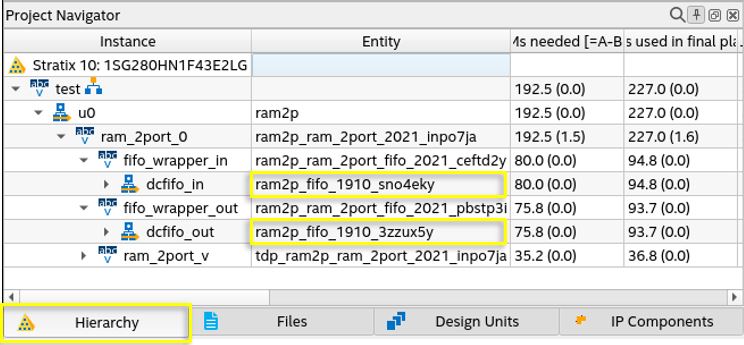
- On the Project Navigator Hierarchy tab, expand your design hierarchy and take note of the entity names of the following instances under the emulated TDP RAM instance:
- Navigate to ram_2port_0 > fifo_wrapper_in > dcfifo_in and take note of the entity name of the dcfifo_in instance.
- Navigate to ram_2port_0 > fifo_wrapper_out > dcfifo_out and take note of the entity name of the dcfifo_out.
Figure 18. Example of dcfifo_in and dcfifo_out Entity Names in the Hierarchy Tab
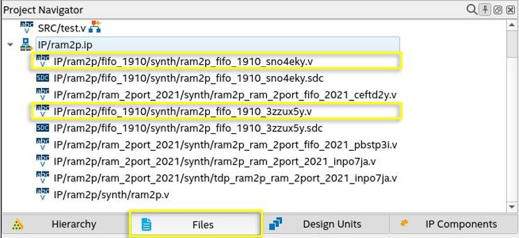
- On the Project Navigator Files tab, expand the .ip file of the emulated TDP RAM and locate <entity name of dcfifo_in>.v and <entity name of dcfifo_out>.v files.
Figure 19. Examples of .ip Files in the Files Tab

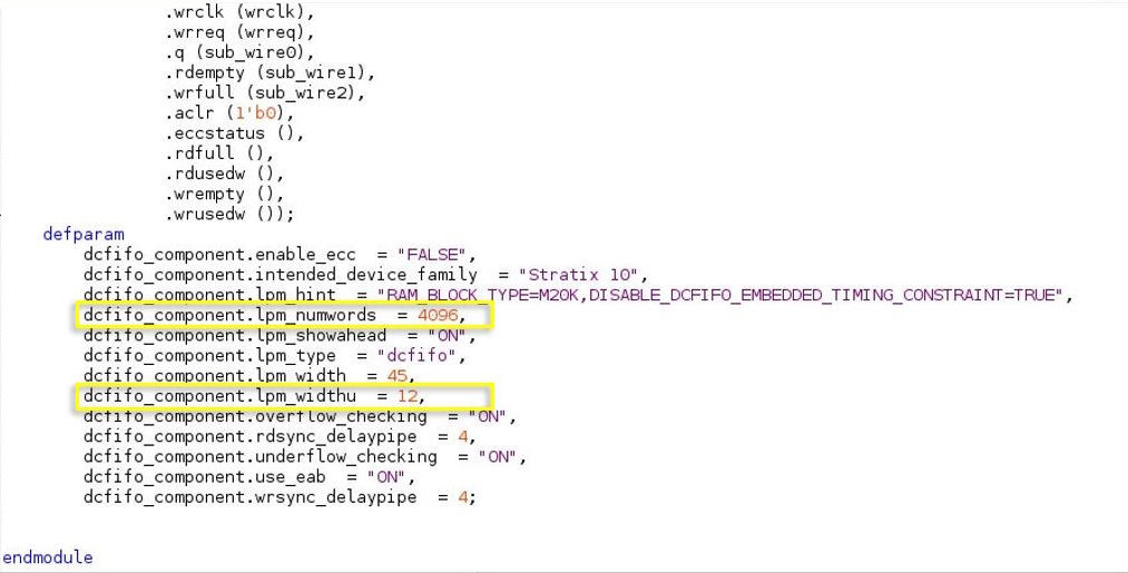
- Click on the <entity names of the dcfifo_in>.v file and find the following parameters in the defparam declarations:
- dcfifo_component.lpm_numwords = <lpm_numwords value>
- dcfifo_component.lpm_widthu = <lpm_widthu value>

- Change the value of dcfifo_component.lpm_numwords and dcfifo_component.lpm_widthu.
- The value of dcfifo_component.lpm_numwords must be greater than the value of the clock frequency ratio of clock B (fast clock) divided by clock A (slow clock) of the emulated TDP RAM IP.
- The value of the dcfifo_component.lpm_numwords must be greater than 4.
- The value of dcfifo_component.lpm_numwords must be the value of 2^dcfifo_component.lpm_widthu. For example:
- If the ratio of the clock B frequency/clock A frequency is 5, the minimum dcfifo_component.lpm_numword must be 8 (2^3).
- If the dcfifo_component.lpm_numword is 8 (2^3), then the value of dcfifo_component.lpm_widthu is 3.
- Save the file. Repeat the same steps for <entity names of the dcfifo_out>.v file of the emulated TDP RAM.
Note: If the emulated TDP RAM IP is regenerated, the above files are regenerated and the parameter values are restored to their default values.