Visible to Intel only — GUID: oly1523608059295
Ixiasoft
1.1. Release Information
1.2. Device Family Support
1.3. Signals
1.4. Parameters
1.5. Register Map
1.6. Using Generic Serial Flash Interface Intel® FPGA IP
1.7. Generic Serial Flash Interface Intel® FPGA IP Reference Design
1.8. Flash Access Using the Generic Serial Flash Interface Intel® FPGA IP
1.9. Nios II HAL Driver
1.10. Generic Serial Flash Interface Intel® FPGA IP User Guide Archives
1.11. Document Revision History for the Generic Serial Flash Interface Intel® FPGA IP User Guide
Visible to Intel only — GUID: oly1523608059295
Ixiasoft
1.7.3. Creating Nios® II Hardware System
- In the Intel® Quartus® Prime software, go to File > New Project Wizard.
- Create a new Intel® Quartus® Prime Prime project named generic_flash_access in a new directory and select the Cyclone V E 5CEFA7F3117 device.
- Select Tools > Platform Designer, and save the file as generic_flash_access.qsys.
- Double-click on the clock source clk_0 and change the Clock frequency to 100000000 Hz (100MHz).
- Right click on clk_0 and rename it as sys_clk.
- Add a Nios® II processor:
- Go to Processor and Peripherals > Embedded Processors > Nios II Processor, and click Add.
- Click Finish to add the Nios® II processor to the design and rename it as nios2.
Note: Ignore any messages about parameters that have not been specified yet.
- Add a Generic Serial Flash Interface IP:
- Select Basic Functions > Configuration and Programming > Generic Serial Flash Interface Intel FPGA IP, and click Add. Rename this component as intel_generic_serial_flash_interface_top0.
- Set the device density.
Note: This reference design uses 1024MB flash device density.
- Connect data_master of processor to avl_mem and avl_csr, and instruction_master of processor to only avl_mem of this component.
- Add an On-chip Memory IP:
- Select Basic Functions > On Chip Memory > On-Chip Memory (RAM or ROM) Intel FPGA IP.
- Set the Total Memory Size to 40960 bytes (40 KBytes).
- Click Finish and rename as main_memory.
- Connect its slave to data_master and instruction_master of processor.
- Add a JTAG UART IP:
- Go to Interface Protocols > Serial > JTAG UART Intel FPGA IP, and click Add.
- Click Finish and rename it as jtag_uart.
- Connect its avalon_jtag_slave port to the data_master port of the processor.
- In the IRQ column, connect the interrupt sender port from the Avalon_jtag_slave port to the interrupt receiver port of the processor and type 0.
- Connect clock input of sys_clk to clock input of all other components.
- Resolve all Nios® II processor error messages before generating the Platform Designer system:
- Double click the Nios® II processor nios2.
- Click Vectors, change both the Reset vector memory and Exception vector memory to main_memory.s1.
- Click System tab and click on the drop-down menu System and click Assign Base Address to auto assign base addresses for all the components.
- Under the same menu, click Create Global Reset Network to connect the reset signals to form a global reset network.
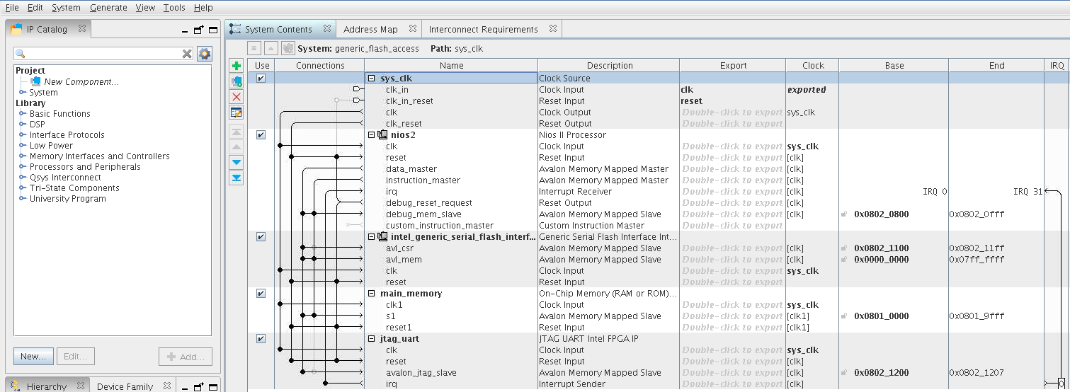
Figure 7. Completed Platform Designer Connection
- Generate the system:
- Click Generate HDL on the bottom of the window.
- When completed, the Platform Designer displays Generate: Completed successfully.