Visible to Intel only — GUID: dyq1591019375315
Ixiasoft
Fixing SDC and CDC Rules in the Design Assistant Design Example
Refer to the intermediate design RTL and SDCs for this section. Compile the design in the intermediate directory to see the effects of all the changes you make in this section.
- Open the design in Quartus® Prime Pro Edition: click File > Open Project and open the base/top.qpf project file from the base directory.
- Under Design Assistant Rule Settings, turn on Enable Design Assistant execution during compilation.
- Compile the design.
- Analyze the results and fix high priority rules first.
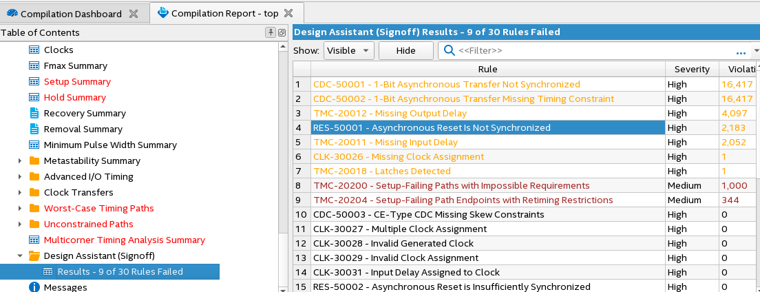
Figure 2. Results in Compilation Mode
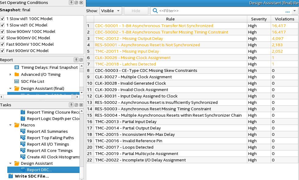
 Figure 3. Results in Analysis Mode in Timing Analyzer
- Update the SDC file and the RTL to fix missing input and output delay constraints for accurate timing results:
- Add missing set_input_delay SDCs to fix TMC-20011.
set_input_delay -add_delay -clock [get_clocks {clk}] 0.500 [get_ports {idat[*]}] -reference_pin [get_pins -no_duplicates {u_top_clk1|wen_q|clk}] set_input_delay -add_delay -clock [get_clocks {clk2}] 0.500 [get_ports {sel[*]}] -reference_pin [get_pins -no_duplicates {u_top_clk2|en0q|clk}] set_input_delay -add_delay -clock [get_clocks {clk}] -min 0.100 [get_ports {idat[*]}] -reference_pin [get_pins -no_duplicates {u_top_clk1|wen_q|clk}] set_input_delay -add_delay -clock [get_clocks {clk2}] -min 0.100 [get_ports {sel[*]}] -reference_pin [get_pins -no_duplicates {u_top_clk2|en0q|clk}] - Add missing set_output_delay SDCs to fix TMC-20012.
set_output_delay -add_delay  -clock [get_clocks {clk}]  -max 0.500 [get_ports {sum[*]}] -reference_pin [get_pins -no_duplicates {u_top_clk1|wen_q|clk}]
set_output_delay -add_delay  -clock [get_clocks {clk}]  -max 0.500 [get_ports {latch_out}] -reference_pin [get_pins -no_duplicates {u_top_clk1|wen_q|clk}]
set_output_delay -add_delay  -clock [get_clocks {clk2}] -max 0.500 [get_ports {final_dat[*]}] -reference_pin [get_pins -no_duplicates {u_top_clk2|en0q|clk}]
set_output_delay -add_delay  -clock [get_clocks {clk}]  -min 0.100 [get_ports {sum[*]}] -reference_pin [get_pins -no_duplicates {u_top_clk1|wen_q|clk}]
set_output_delay -add_delay  -clock [get_clocks {clk}]  -min 0.100 [get_ports {latch_out}] -reference_pin [get_pins -no_duplicates {u_top_clk1|wen_q|clk}]
set_output_delay -add_delay  -clock [get_clocks {clk2}] -min 0.100 [get_ports {final_dat[*]}] -reference_pin [get_pins -no_duplicates {u_top_clk2|en0q|clk}]
Refer to Timing Closure Rules for more information about these and other related rules. - Add missing set_input_delay SDCs to fix TMC-20011.
- Add reset synchronizers to fix RES-50001.
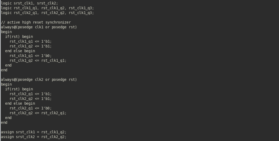
- In top.sv, add reset synchronization logic and feed their outputs to their respective clock domain to prevent metastability.
Figure 4. RES-50001

- Constrain the new reset synchronizers or you see violations on RES-50003 or you may see violations on RES-50003 on subsequent compilations. Add false paths to the clrn pins of the reset synchronizer.
set_false_path -from [get_ports rst] -to [get_pins rst_clk1_q1|clrn]
set_false_path -from [get_ports rst] -to [get_pins rst_clk1_q2|clrn]
set_false_path -from [get_ports rst] -to [get_pins rst_clk2_q1|clrn]
set_false_path -from [get_ports rst] -to [get_pins rst_clk2_q2|clrn]
- In top.sv, add reset synchronization logic and feed their outputs to their respective clock domain to prevent metastability.
- Add synchronization logic for data going between clk1 and clk2 and vice versa by changing top.sv and top_clk2.sv. The following code shows the CDC for going from clk1 to clk2.
// top.sv // generate a pulse in one clock domain always@(posedge clk1) en_q <= en; // detect the positive edge of the pulse and change edges // this edge crosses the clock domain always@(posedge clk1 or posedge srst_clk1) begin if(srst_clk1) en_pulse_det0q <= 1'b0; else if(en & ~en_q) en_pulse_det0q <= !en_pulse_det0q; end // send en_pulse_det0q into the en input of top_clk2.sv // top_clk2.sv: logic en2_pulse; logic en0q, en1q, en2q; // synchronize the detected edge into the clk2 domain and use it // to generate a pulse always@(posedge clk2) begin en0q <= en; en1q <= en0q; en2q <= en1q; en2_pulse <= en2q ^ en1q; end // use the pulse to enable data capture always@(posedge clk2) begin if(en2_pulse) idat_q <= idat;- Add SDCs to constrain the CDC correctly. Rules CDC-50002 and CDC-50003 detect missing SDCs.
set_clock_groups -asynchronous -group {clk} -group {clk2}

# clk1 to clk2 paths
for {set i 0} {$i < 8 } {incr i} {
set_net_delay -from u_top_clk1|[$i].u_byte_enabled_simple_dual_port_ram_out|* -to u_top_clk2|idat_q[$i][*] -max \
   -get_value_from_clock_period dst_clock_period -value_multiplier 0.8
set_max_skew -from u_top_clk1|[$i].u_byte_enabled_simple_dual_port_ram_out|*  -to u_top_clk2|idat_q[$i][*] \
   -get_skew_value_from_clock_period src_clock_period -skew_value_multiplier 0.8
}

# clk2 to clk1 paths
set_net_delay -from u_top_clk2|math_q[*] -to math2_clk1[*] -max \
   -get_value_from_clock_period dst_clock_period -value_multiplier 0.8
set_max_skew -from u_top_clk2|math_q[*] -to math2_clk1[*] \
   -get_skew_value_from_clock_period src_clock_period -skew_value_multiplier 0.8
Refer to Clock Domain Crossing and Reset Domain Crossing Rule for more information about these and other related rules.
- Add SDCs to constrain the CDC correctly. Rules CDC-50002 and CDC-50003 detect missing SDCs.
- Remove inferred latch in RTL. Rule TMC-20018 catches the latch. Rule CLK-30026 catches that the design is using the en signal as a clock for the inferred latch.
// TMC-20018 inferred latch; CLK-30026 flags the en signal as a clock
logic inferred_lat;
always@(*) begin
  if(en)
    inferred_lat <= math1[0];
end
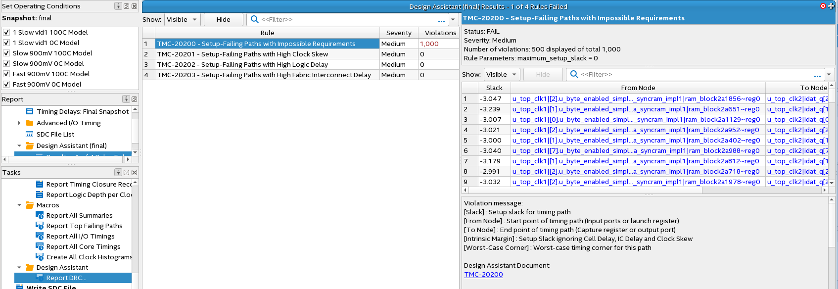
The fix is:// latch logic inferred_lat; always@(posedge clk1) begin if(en) inferred_lat <= math1[0]; end - In the base design, check for any TMC-20200 and TMC-20201 rule failures, which may be due to incorrect SDCs and improper CDCs. However, the fixes made in the previous steps should resolve them in this example design.
Refer to Intrinsic Margin for more information on these and other related rules.Figure 5. TMC-20200 Rule Violations
