Intel® Stratix® 10 GX Transceiver Signal Integrity Development Kit User Guide
ID
683206
Date
2/21/2023
Public
Visible to Intel only — GUID: fli1472853893181
Ixiasoft
6.3.1. The Configure Menu
To configure the FPGA with a test system design, perform the following steps:
6.3.2. The System Info Tab
6.3.3. The GPIO Tab
6.3.4. The Flash Tab
6.3.5. The FMCA Tab
6.3.6. The FMCB Tab
6.3.7. The LPBK Tab
6.3.8. The MXP Tab
6.3.9. The SMA Tab
6.3.10. The QSFP and SFP+ Tab
6.3.11. The CFP4 Tab
6.3.12. Power Monitor
6.3.13. Clock Controller
Visible to Intel only — GUID: fli1472853893181
Ixiasoft
6.3.1. The Configure Menu
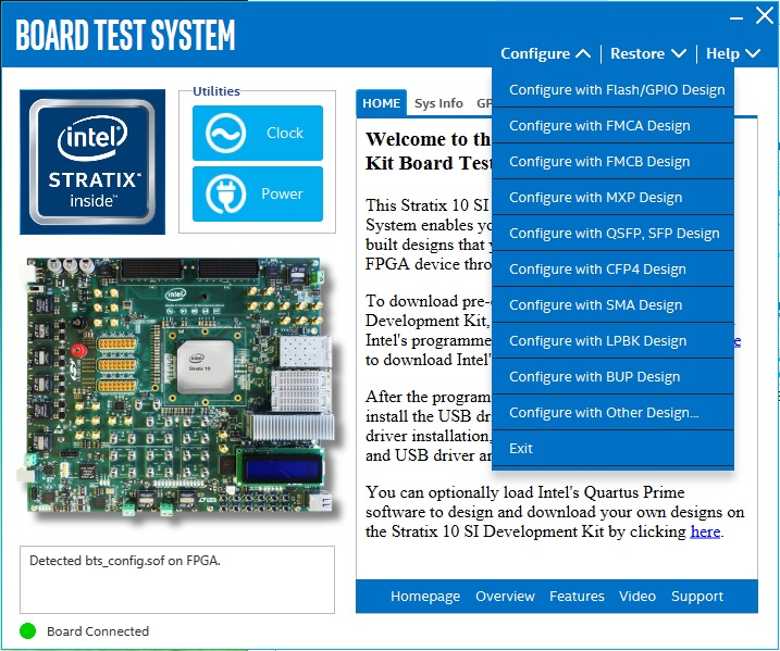
Use the Configure Menu to select the design you want to use. Each design example tests different functionality that corresponds to one or more application tabs.
Figure 16. The Configure Menu


To configure the FPGA with a test system design, perform the following steps:
- On the Configure Menu, click the configure command that corresponds to the functionality you wish to test.
- In the dialog box that appears, click Configure to download the corresponding design's SRAM Object File (.sof) to the FPGA. The download process usually takes less than a minute.
- When configuration finishes, the design begins running in the FPGA. The corresponding GUI application tabs that interface with the design are now enabled. If you use the Intel® Quartus® Prime Programmer for configuration, rather than the BTS GUI, you may need to restart the GUI.