3.1. Synthesis Design Example
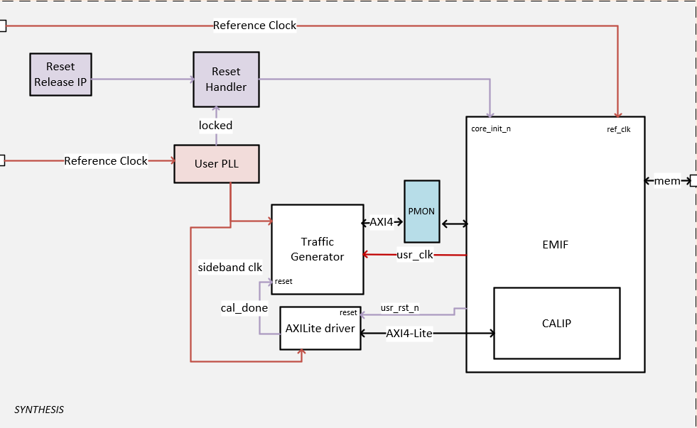
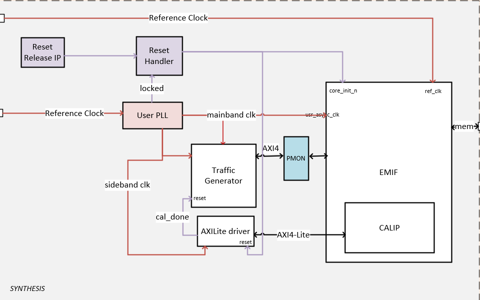
The synthesis design example contains the major blocks described below.
- A traffic generator is a synthesizable AXI4 driver that implements a hard-coded pattern and monitors the data read from the memory to ensure that it matches the written data, and asserts a failure otherwise. You can select different traffic generator programs when generating the example design. Each program performs the following transactions:
- Single write and read (with AxLEN=axlen_a 1 ) 2
- Single write and read (with AxLEN=axlen_b 1 ) 2
- Sequential address 3 block of m 4 writes and m 4 reads (with AxLEN=axlen_a 1 )
- Sequential address 3 block of m 4 writes and m 4 reads (with AxLEN=axlen_b 1 )
- Random address 5 block of m 4 writes and m 4 reads (with AxLEN=axlen_a 1 )
1 The axlen_a and axlen_b values depend on the memory technology. 2 Repeated for 3 loops in the traffic generator program = Short. 3 Sequential Address pattern starts at address=0, and increments by (AXI_DATA_WIDTH/8)*(AxLEN+1) on each transaction. 4 The m value depends on the traffic generator program. 5 Random address pattern starts at address=0, and uses pseudo-random addresses. Table 13. axlen_a and axlen_b for Different memory Technologies Technology axlen_a axlen_b Notes DDR4 0 0 DDR5 1 0 axlen_b=0 results in Read-Modify-Write or data-masking on the memory side. LPDDR4 3 3 LPDDR5 1 1 Table 14. m value in Different Traffic Generator programs Traffic Generator Program m Short 128 Medium 512 Long 4096 - An instance of the memory interface, which includes:
- A memory controller which implements all the memory commands and protocol-level requirements.
- The PHY, which serves as an interface between the memory controller and external memory devices to perform read and write operations.
Figure 21. Synthesis Design Example Sync Fabric Mode


Figure 22. Synthesis Design Example Async Fabric Mode


You must add the following assignment to the .qsf file to allow for less-restricted placement of the user PLL:
set_instance_assignment –name PLL_REFCLK_INPUT_TYPE NOT_BALANCED -to user_pll|altera_iopll_inst
If a user PLL shares an I/O bank with EMIF, you may additionally need to specify an operating voltage I/O standard. The voltage of the pin depends on the operating voltage of the EMIF occupying that bank, which, in turn, depends on the memory protocol, as follows:
- DDR4 = 1.2V
- DDR5 = 1.1V
- LPDDR4 = 1.1V
- LPDDR5 = 1.05V
For example, for a PLL whose reference clock is in the same bank as an LPDDR4 EMIF, the assignment show look like this:
set_instance_assignment -name IO_STANDARD "1.1V True Differential Signaling" -to "ref_clk_usr_pll"