A newer version of this document is available. Customers should click here to go to the newest version.
Visible to Intel only — GUID: zpm1684717282083
Ixiasoft
1. Agilex™ 5 Embedded Memory Overview
2. Agilex™ 5 Embedded Memory Architecture and Features
3. Agilex™ 5 Embedded Memory Design Considerations
4. Agilex™ 5 Embedded Memory IP References
5. Agilex™ 5 Embedded Memory Debugging
6. Embedded Memory User Guide: Agilex™ 5 FPGAs and SoCs Archives
7. Document Revision History for the Embedded Memory User Guide: Agilex™ 5 FPGAs and SoCs
2.1. Byte Enable in Agilex™ 5 Embedded Memory Blocks
2.2. Address Hold Support
2.3. Asynchronous Clear and Synchronous Clear
2.4. Memory Blocks Error Correction Code (ECC) Support
2.5. Agilex™ 5 Embedded Memory Clocking Modes
2.6. Agilex™ 5 Embedded Memory Configurations
2.7. Force-to-Zero
2.8. Coherent Read Memory
2.9. Freeze Logic
2.10. True Dual Port Dual Clock Emulator
2.11. Initial Value of Read and Write Address Registers
2.12. Timing/Power Optimization Feature in M20K Blocks
3.1. Consider the Memory Block Selection
3.2. Consider the Concurrent Write Behavior
3.3. Read-During-Write (RDW)
3.4. Consider Power-Up State and Memory Initialization
3.5. Reduce Power Consumption
3.6. Avoid Providing Non-Deterministic Input
3.7. Avoid Changing Clock Signals and Other Control Signals Simultaneously
3.8. Advanced Settings in Quartus® Prime Software for Memory
3.9. Consider the Memory Depth Setting
3.10. Consider Registering the Memory Output
4.1.4.1. RAM: 1-PORT Intel® FPGA IP Parameters
4.1.4.2. RAM: 2-PORT Intel® FPGA IP Parameters
4.1.4.3. RAM: 4-PORT Intel® FPGA IP Parameters
4.1.4.4. ROM: 1-PORT Intel® FPGA IP Parameters
4.1.4.5. ROM: 2-PORT Intel® FPGA IP Parameters
4.1.4.6. RAM and ROM Parameter Settings
4.1.4.7. Changing Parameter Settings Manually
4.1.4.8. RAM and ROM Interface Signals
4.2.5.1. FIFO Functional Timing Requirements
4.2.5.2. SCFIFO ALMOST_EMPTY Functional Timing
4.2.5.3. FIFO Output Status Flag and Latency
4.2.5.4. FIFO Metastability Protection and Related Options
4.2.5.5. FIFO Synchronous Clear and Asynchronous Clear Effect
4.2.5.6. SCFIFO and DCFIFO Show-Ahead Mode
4.2.5.7. Different Input and Output Width
4.2.5.8. DCFIFO Timing Constraint Setting
4.2.5.9. Gray-Code Counter Transfer at the Clock Domain Crossing
4.2.5.10. Guidelines for Embedded Memory ECC Feature
4.2.5.11. Reset Scheme
Visible to Intel only — GUID: zpm1684717282083
Ixiasoft
4.2.3.2.4. HDL Code from Parameterizable Macros Template
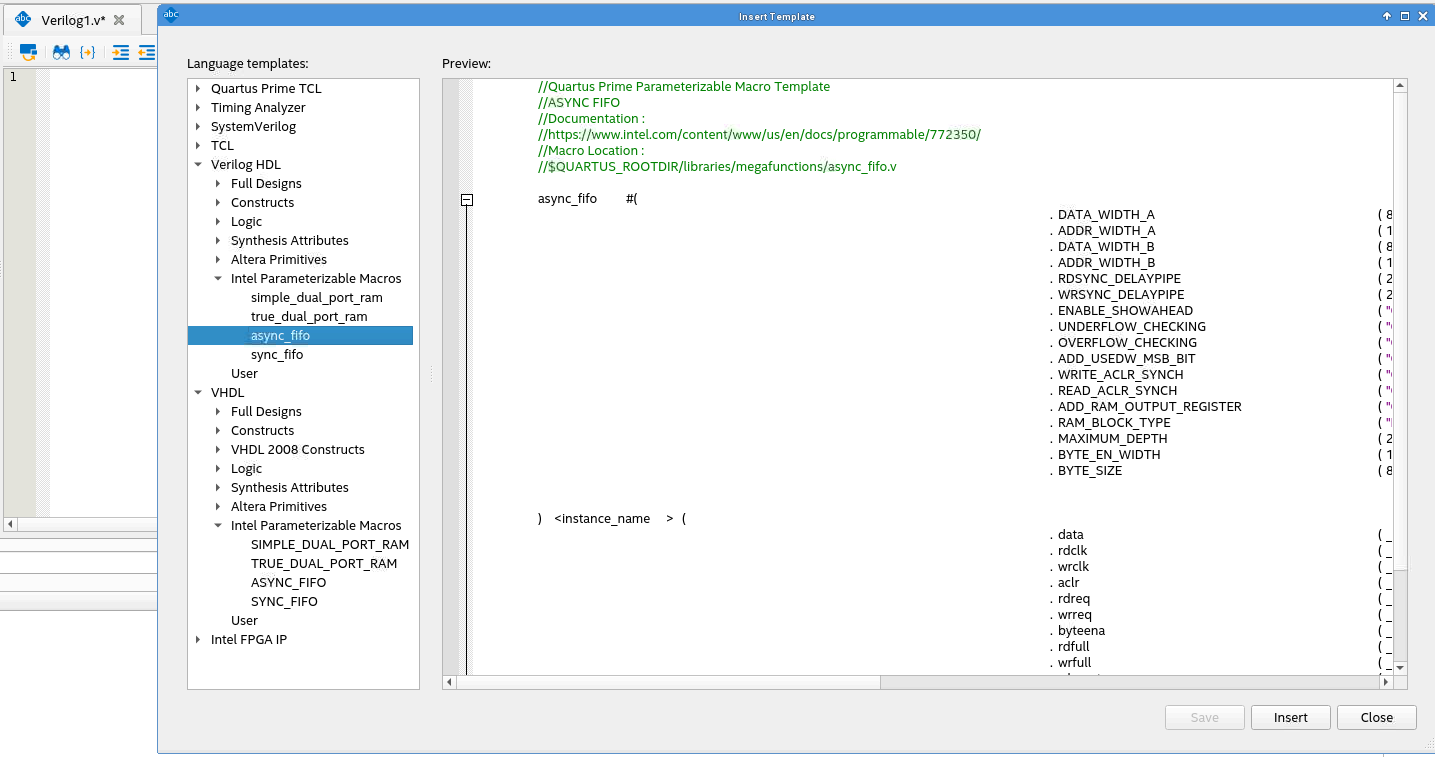
Alternatively, you can utilize the Verilog HDL or VHDL code from the Parameterizable Macros template.
- Right-click the HDL file and select Insert Template.
- In the Insert Template dialog box, select Verilog HDL or VHDL and select Intel Parameterizable Macros.
- Select from the available templates and click Insert.
Figure 32. Inserting a Parameterizable Macros Template