Visible to Intel only — GUID: bbj1660068408214
Ixiasoft
Visible to Intel only — GUID: bbj1660068408214
Ixiasoft
3.2. Simulation Design Example
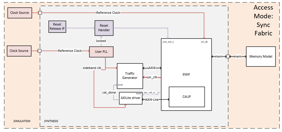
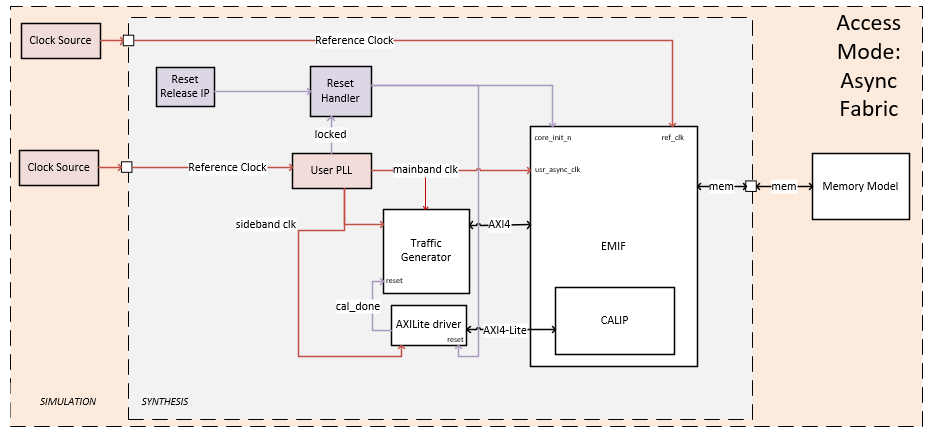
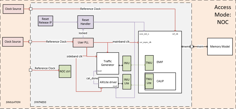
- An instance of the synthesis design example. As described in the previous section, the synthesis design example contains a traffic generator and an instance of the memory interface.
- A memory model, which acts as a generic model that adheres to the memory protocol specifications. Frequently, memory vendors provide simulation models for their specific memory components that you can download from their websites.


You must add the following assignment to the .qsf file to allow for less-restricted placement of the user PLL:
set_instance_assignment –name PLL_REFCLK_INPUT_TYPE NOT_BALANCED -to user_pll|altera_iopll_inst
If a user PLL shares an I/O bank with EMIF, you may additionally need to specify an operating voltage I/O standard. The voltage of the pin depends on the operating voltage of the EMIF occupying that bank, which, in turn, depends on the memory protocol, as follows:
- DDR4 = 1.2V
- DDR5 = 1.1V
- LPDDR5 = 0.7V
For example, for a PLL whose reference clock is in the same bank as a DDR5 EMIF, the assignment show look like this:
set_instance_assignment -name IO_STANDARD "1.1V True Differential Signaling" -to "ref_clk_usr_pll"