Visible to Intel only — GUID: lup1660068391969
Ixiasoft
1. About the External Memory Interfaces Intel Agilex® 7 M-Series FPGA IP
2. Design Example Quick Start Guide for External Memory Interfaces Intel Agilex® 7 M-Series FPGA IP
3. Design Example Description for External Memory Interfaces Intel Agilex® 7 M-Series FPGA IP
4. Document Revision History for External Memory Interfaces Intel Agilex® 7 M-Series FPGA IP Design Example User Guide
2.1. Creating an EMIF Project
2.2. Generating and Configuring the EMIF IP
2.3. Configuring DQ Pin Swizzling
2.4. Generating the Synthesizable EMIF Design Example
2.5. Generating the EMIF Design Example for Simulation
2.6. Pin Placement for Intel Agilex® 7 M-Series EMIF IP
2.7. Compiling the Intel Agilex® 7 M-Series EMIF Design Example
2.1.1.3.1. Generating a Custom Memory Preset File for DDR4
2.1.1.3.2. Guidelines for Selecting the DDR4 DRAM Component Package Type
2.1.1.3.3. Generating a Custom Memory Preset File for DDR5
2.1.1.3.4. Guidelines for Selecting the DDR5 DRAM Component Package Type
2.1.1.3.5. Generating a Custom Memory Preset File for LPDDR5
Visible to Intel only — GUID: lup1660068391969
Ixiasoft
3.1. Synthesis Design Example
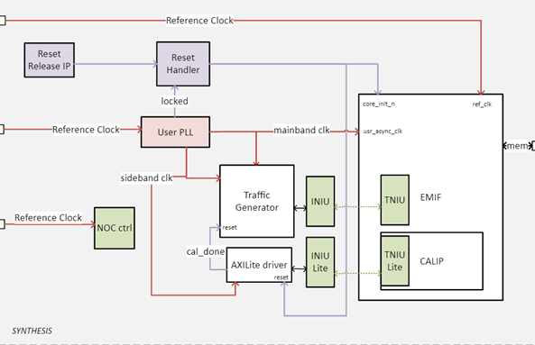
The synthesis design example contains the major blocks shown in the figure below.
- A traffic generator, which is a synthesizable AXI4 driver that implements a hard-coded pattern. The traffic generator also monitors the data read from the memory to ensure it matches the written data and asserts a failure otherwise.
- Single write and read (with AxLEN=axlen_a 1 )
- Single write and read (with AxLEN=axlen_b 2 )
- Sequential address 3 block of 512 writes and 512 reads (with AxLEN=axlen_a 1 )
- Sequential address 3 block of 512 writes and 512 reads (with AxLEN=axlen_b 2 )
- Random address 4 block of 512 writes and 512 reads (with AxLEN= axlen_a 1 )
1 The axlen_a value is dependent on the memory technology: - For DDR4: 0
- For DDR5: 1
- For LPDDR5: 3
2 The axlen_b value is dependent on the memory technology: - For DDR4: 0
- For DDR5: 0 (results in Read-Modify-Write or Data-Masking on the memory side).
- For LPDDR5: 3
3 Sequential Address pattern starts at address=0, and increments by (AXI_DATA_WIDTH/8)*(AxLEN+1) on each transaction. 4 Random Address pattern starts at address=0, and uses pseudo-random addresses. - An instance of the memory interface, which includes:
- A memory controller which implements all the memory commands and protocol-level requirements.
- The PHY, which serves as an interface between the memory controller and external memory devices to perform read and write operations.
Figure 35. Synthesis Design Example Sync Fabric Mode
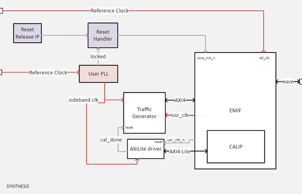

Figure 36. Synthesis Design Example Async Fabric Mode
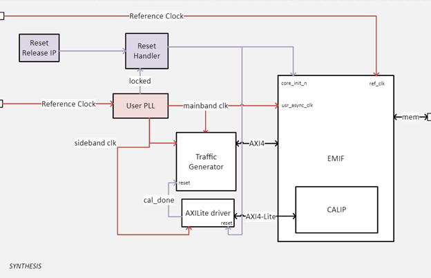

Figure 37. Synthesis Design Example NoC Fabric Mode
