Visible to Intel only — GUID: fcw1685448854850
Ixiasoft
1. About the External Memory Interfaces Intel Agilex® 7 M-Series FPGA IP
2. Intel Agilex® 7 M-Series FPGA EMIF IP – Introduction
3. Intel Agilex® 7 M-Series FPGA EMIF IP – Product Architecture
4. Intel Agilex® 7 M-Series FPGA EMIF IP – End-User Signals
5. Intel Agilex® 7 M-Series FPGA EMIF IP – Simulating Memory IP
6. Intel Agilex 7 M-Series FPGA EMIF IP – DDR4 Support
7. Intel Agilex® 7 M-Series FPGA EMIF IP – DDR5 Support
8. Intel Agilex 7 M-Series FPGA EMIF IP – LPDDR5 Support
9. Intel Agilex® 7 M-Series FPGA EMIF IP – Timing Closure
10. Intel Agilex® 7 M-Series FPGA EMIF IP – Controller Optimization
11. Intel Agilex® 7 M-Series FPGA EMIF IP – Debugging
12. Document Revision History for External Memory Interfaces Intel Agilex® 7 M-Series FPGA IP User Guide
3.1.1. Intel Agilex® 7 M-Series EMIF Architecture: I/O Subsystem
3.1.2. Intel Agilex® 7 M-Series EMIF Architecture: I/O SSM
3.1.3. Intel Agilex® 7 M-Series EMIF Architecture: I/O Bank
3.1.4. Intel Agilex® 7 M-Series EMIF Architecture: I/O Lane
3.1.5. Intel Agilex® 7 M-Series EMIF Architecture: Input DQS Clock Tree
3.1.6. Intel Agilex® 7 M-Series EMIF Architecture: PHY Clock Tree
3.1.7. Intel Agilex® 7 M-Series EMIF Architecture: PLL Reference Clock Networks
3.1.8. Intel Agilex® 7 M-Series EMIF Architecture: Clock Phase Alignment
3.1.9. User Clock in Different Core Access Modes
Benefits of Each Access Mode
6.2.4.1. Address and Command Pin Placement for DDR4
6.2.4.2. DDR4 Data Width Mapping
6.2.4.3. General Guidelines - DDR4
6.2.4.4. x4 DIMM Implementation
6.2.4.5. Specific Pin Connection Requirements
6.2.4.6. Command and Address Signals
6.2.4.7. Clock Signals
6.2.4.8. Data, Data Strobes, DM/DBI, and Optional ECC Signals
6.3.5.1. Single Rank x 8 Discrete (Component) Topology
6.3.5.2. Single Rank x 16 Discrete (Component) Topology
6.3.5.3. ADDR/CMD Reference Voltage/RESET Signal Routing Guidelines for Single Rank x 8 and Single Rank x 16 Discrete (Component) Topologies
6.3.5.4. Skew Matching Guidelines for DDR4 Discrete Configurations
6.3.5.5. Power Delivery Recommendations for DDR4 Discrete Configurations
6.3.5.6. Intel Agilex® 7 M-Series EMIF Pin Swapping Guidelines
7.2.1. Intel Agilex® 7 M-Series FPGA EMIF IP Interface Pins
7.2.2. Intel Agilex® 7 M-Series FPGA EMIF IP Resources
7.2.3. Pin Guidelines for Intel Agilex® 7 M-Series FPGA EMIF IP
7.2.4. Pin Placements for Intel Agilex 7 M-Series FPGA DDR5 EMIF IP
7.2.5. Intel Agilex® 7 M-Series EMIF Pin Swapping Guidelines
Visible to Intel only — GUID: fcw1685448854850
Ixiasoft
3.1.9. User Clock in Different Core Access Modes
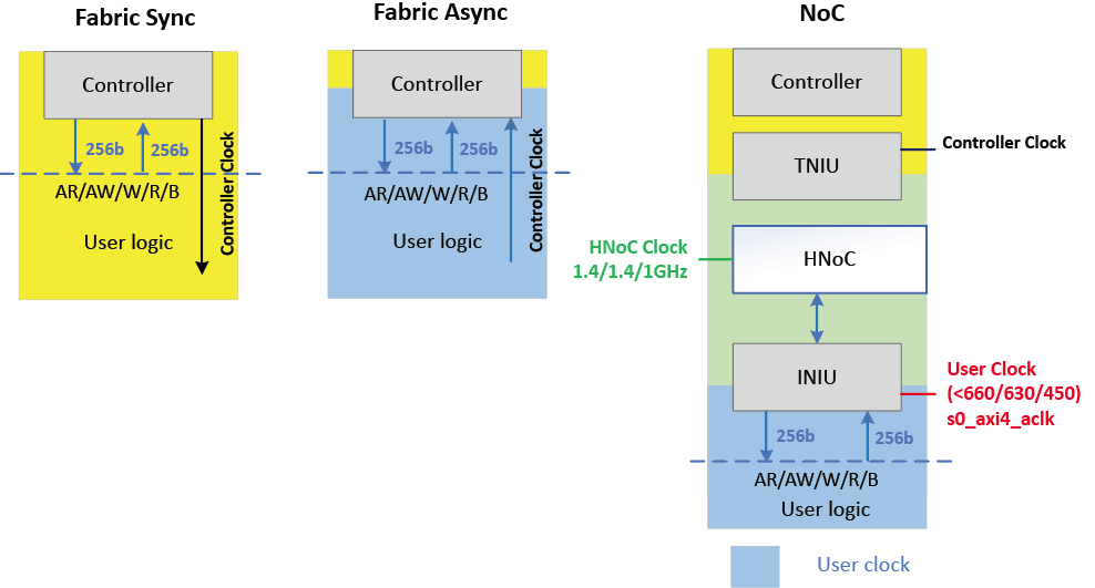
The EMIF IP for Intel Agilex® 7 M-Series devices supports three user access modes.
- Synchronous fabric clocking, where the EMIF IP provides a user clock.
- The user clock frequency is limited by the maximum core-to-periphery (C2P) and periphery-to-core (P2) frequency of 400 MHz.
- In DDR4, the user clock frequency will be one-quarter of the memory clock frequency ((mem_CK)/4).
- In DDR5 and LPDDR5, the user clock frequency will be one-eighth of the memory clock frequency ((mem CK)/8).
- Asynchronous fabric clocking, where you provide the clock to the EMIF IP.
- The asynchronous user clock can come from any user clock source on the device.
- The user clock frequency has no dependency on the memory clock (mem_CK).
- NoC Mode.
- The initiator clock can come from any user clock source on the device.
- For additional information, refer to the Intel Agilex® 7 M-Series FPGA Network-on-Chip (NoC) User Guide .
The following figures illustrate the different clocking styles available for the Intel Agilex® 7 M-Series EMIF IP. The NoC mode shown is the simplest NoC mode.
Figure 10. Access Modes


Benefits of Each Access Mode
- Synchronous fabric clocking is required for DDR4 DIMM.
- Asynchronous fabric access mode has the lowest latency.
- NoC mode can achieve the highest bandwidth and efficiency, and has the lowest initiator blockage.