Visible to Intel only — GUID: ddz1678993619998
Ixiasoft
1. Intel® FPGA AI Suite SoC Design Example User Guide
2. About the SoC Design Example
3. Intel® FPGA AI Suite SoC Design Example Quick Start Tutorial
4. Intel® FPGA AI Suite SoC Design Example Run Process
5. Intel® FPGA AI Suite SoC Design Example Build Process
6. Intel® FPGA AI Suite SoC Design Example Intel® Quartus® Prime System Architecture
7. Intel® FPGA AI Suite Soc Design Example Software Components
8. Streaming-to-Memory (S2M) Streaming Demonstration
A. Intel® FPGA AI Suite SoC Design Example User Guide Archives
B. Intel® FPGA AI Suite SoC Design Example User Guide Document Revision History
3.1. Initial Setup
3.2. Initializing a Work Directory
3.3. (Optional) Create an SD Card Image (.wic)
3.4. Writing the SD Card Image (.wic) to an SD Card
3.5. Preparing SoC FPGA Development Kits for the Intel® FPGA AI Suite SoC Design Example
3.6. Adding Compiled Graphs (AOT files) to the SD Card
3.7. Verifying FPGA Device Drivers
3.8. Running the Demonstration Applications
3.5.1.1. Confirming Intel Agilex® 7 FPGA I-Series Transceiver-SoC Development Kit Board Set Up
3.5.1.2. Programming the Intel Agilex® 7FPGA Device with the JTAG Indirect Configuration (.jic) File
3.5.1.3. Connecting the Intel Agilex® 7 FPGA I-Series Transceiver-SoC Development Kit to the Host Development System
7.1.1. Yocto Recipe: recipes-core/images/coredla-image.bb
7.1.2. Yocto Recipe: recipes-bsp/u-boot/u-boot-socfpga_%.bbapend
7.1.3. Yocto Recipe: recipes-drivers/msgdma-userio/msgdma-userio.bb
7.1.4. Yocto Recipe: recipes-drivers/uio-devices/uio-devices.bb
7.1.5. Yocto Recipe: recipes-kernel/linux/linux-socfpga-lts_5.15.bbappend
7.1.6. Yocto Recipe: wic
Visible to Intel only — GUID: ddz1678993619998
Ixiasoft
6.4. Top Level
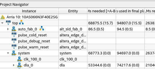
After the Intel® Quartus® Prime project has finished executing, the design should look similar to the following image in the Intel® Quartus® Prime Project Navigator:
Figure 10. SoC Design Example Hierarchy
The top-level Verilog file and HPS configuration is derived directly from the GSRD designs located at RocketBoards.org:
- For more information about the GSRD for the Intel Agilex® 7 FPGA I-Series Transceiver-SoC Development Kit, refer to the following URL https://www.rocketboards.org/foswiki/Documentation/AgilexSoCGSRDSIAGI027
- For more information about the GSRD for the Intel® Arria® 10 SX SoC FPGA Development Kit, refer to the following URL: https://www.rocketboards.org/foswiki/Documentation/arria10SoCGSRD
The GSRD designs have been modified to include the Intel® FPGA AI Suite IP. All unnecessary logic has been removed, which provides a concise design example.
The main Intel® FPGA AI Suite SoC design example is contained within a single Platform Designer system, called system. Double-click this node in the Intel® Quartus® Prime Project Navigator to launch Platform Designer.