Visible to Intel only — GUID: ptq1619516629947
Ixiasoft
Visible to Intel only — GUID: ptq1619516629947
Ixiasoft
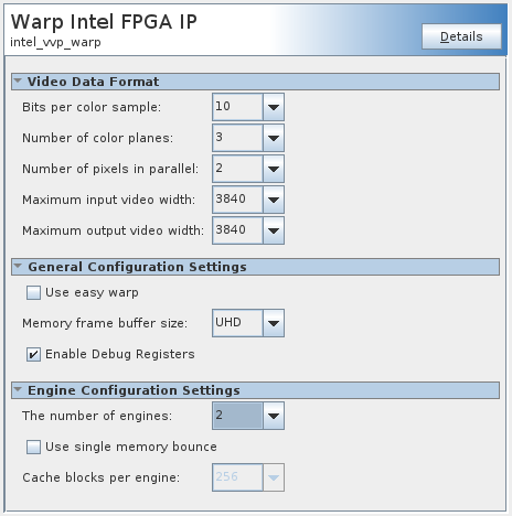
49.2. Warp IP Parameters
| Parameter | Values | Description |
|---|---|---|
| Video data format | ||
| Number of pixels in parallel | 1 or 2 | Number of pixels processed in parallel. |
| Number of color planes | 3 | Number of color planes per pixel. |
| Bits per color sample | 10 | Number of bits per color sample |
| Maximum input video width | 2048 or 3840 | Maximum number of pixels per input line. Configures the depth of line buffers in the video input block. The IP can process image widths of up to 3840. However, it can process only horizontal resolutions that are a multiple of 4 pixels. For example, the IP can process image widths of 720 or 724 correctly but not widths of 721, 722 or 723. |
| Maximum output video width | 2048 or 3840 | Maximum number of pixels per output line. Configures the depth of line buffers in the video output block. |
| Configuration Settings | ||
| Use easy warp | On or off | Turn on for a limited set of warp operations. Turn off for a range of arbitrary warps. The IP can only process image heights and widths that are a multiple of two when you select 2 pixels in parallel and turn on Use easy warp. |
| Memory frame buffer size | SD, HD or UHD | The amount of memory space the IP allocates to each frame buffer.
|
| Enable Debug Registers | On or off | Turn on to read back various registers containing debugging information. |
| Engine Configuration Settings (These parameters are only available when Use easy warp is off) |
||
| Number of engines | 1 or 2 | Number of processing engines to use. Each engine processes one pixel per clock cycle. |
| Use single memory bounce | On or off | Defines how the engines are connected to and use the external memory. When you turn off Use single memory bounce the engines both read and write their video data through the memory (double memory bounce). When you turn on Use single memory bounce the engines only read video data from memory and their output data passes directly to the video output process of the warp IP. The IP can only generate image heights that are a multiple of 8 lines when you turn on Use single memory bounce. |
| Cache blocks per engine | 256, 512 or 1024 | Only available when Use single memory bounce is on. Defines the amount of cache memory that is available to each engine. The amount of cache memory required is a function of the input resolution the IP processes, the required warp and the number of engines you select. |

| Number of pixels in parallel | The number of processing engines to use | fMAX (MHz) | Performance |
|---|---|---|---|
| 1 | 1 | 150 | Image resolutions of up to 1920x1080 at 60 fps. |
| 1 | 1 | 300 | Image resolutions of up to 3840x2160 at 30 fps. |
| 2 | 2 | 300 | Image resolutions of up to 3840x2160 at 60 fps. |
| 1 | 1 | 600 | Image resolutions of up to 3840x2160 at 60 fps. |