Visible to Intel only — GUID: opc1596130839784
Ixiasoft
Visible to Intel only — GUID: opc1596130839784
Ixiasoft
4.4.8.1. Completion Buffer Size
P-tile Hard IP for PCIe implements Completion (Cpl) buffers for header and data for each PCIe core. In Endpoint mode, when Completion credits are infinite, user application needs to manage the number of outstanding requests to prevent overflow and lost Completions.
| Completion Buffer | Depth (in Numbers of Credits) | Width (in Bits) |
|---|---|---|
| Port 0 Cpl header | 1144 | NA |
| Port 0 Cpl data | 1444 | 256 |
| Port 1 Cpl header | 572 | NA |
| Port 1 Cpl data | 1444 | 128 |
| Port 2 Cpl header | 286 | NA |
| Port 2 Cpl data | 1444 | 64 |
| Port 3 Cpl header | 286 | NA |
| Port 3 Cpl data | 1444 | 64 |
Application Layer should send a request when there are sufficient completion buffer entries.
For Memory Read request, the Completer is allowed to break up the response for a single Read Request into multiple Completions, so Application Layer needs to account for the maximum possible Completions returned.
Below are a few examples for the amount of Completion buffer entries that would be required based on the Memory Read request size and the Read Completion Boundary (RCB) configuration.
| Memory Read Request Examples | Completion Buffer Entries Required | |||||
|---|---|---|---|---|---|---|
| Port 0 | Port 1 | Port 2/3 | ||||
| Header | Data | Header | Data | Header | Data | |
A Memory Read request with an address of 1_0000h and length of C0h bytes (192 decimal) can be completed by a Root Complex with an RCB value of 64 bytes with one of the following combinations of Completions (bytes):
|
3 | 6 | 3 | 12 | 3 | 24 |
A Memory Read request with an address of 1_0000h and length of C0h bytes (192 decimal) can be completed by a Root Complex with an RCB value of 128 bytes with one of the following combinations of Completions (bytes):
|
2 | 6 | 2 | 12 | 2 | 24 |
A Memory Read request with an address of 1_0020h and length of 100h bytes (256 decimal) can be completed by a Root Complex with an RCB value of 64 bytes with one of the following combinations of Completions (bytes):
|
5 | 8 | 5 | 16 | 5 | 32 |
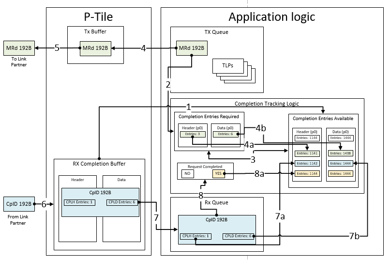
Based on the examples from the table above, Suggested Flow for Application Logic to Track Completion Buffer Entries and Schedule NP Requests to P-tile IP for PCIe below provides the suggested flow in the Application logic to track the completion buffer entries and based on this, schedule Non-Posted (NP) requests to the P-Tile Intel FPGA IP for PCI Express.
For illustration purposes, Suggested Flow for Application Logic to Track Completion Buffer Entries and Schedule NP Requests to P-tile IP for PCIe is showing the P-Tile Intel FPGA IP for PCIe express configured in Gen4 x16 (Port 0), with the Application logic requesting a Memory Read of 192 Bytes and getting a single completion of 192 Bytes in the response from the link partner.
- When dl_up signal goes from LOW to HIGH, the Application logic initializes the available completion buffer entries based on CPL buffer size table above from Completion Buffer Size.
- When there is an NP request added to transmission queue of the Application logic, the Completion Tracking logic calculates the required completion buffer entries for the request, considering the maximum number of completions that could be received. For this example, it is 3 completions of 64 Bytes. (Refer to the table with the examples provided in Memory Read Request Examples).
- The Completion Tracking logic checks the required completion buffer entries against the available completion buffer entries.
- If there are sufficient buffer entries available, the Application logic schedules the Memory Read request for transmission.
- The Completion Tracking logic updates the available completion header buffer entries.
- The Completion Tracking logic updates the available completion data buffer entries.
- The P-Tile Intel FPGA IP for PCI Express sends the NP TLP to the link partner.
- The link partner responds to the MRd request with a single Completion with a data payload of 192B.
- When the Completion packet is received by the Application Layer in its Rx Queue,
- The Completion Tracking logic updates the available completion header buffer entries.
- The Completion Tracking logic updates the available completion data buffer entries.
- The Completion Tracking logic verifies if the original NP request has been fully completed with the Completion received.
- If the request has been completed, the Completion Tracking logic adjusts the available completion buffer entries based on the unused entries allocated to the request previously.
- In case of multiple Completions for steps 8 and 8a, the Completion Tracking Logic will update the completion buffer entries for each Completion TLP received accordingly.
