External Memory Interfaces (EMIF) IP User Guide: Agilex™ 3 FPGAs and SoCs
Visible to Intel only — GUID: ppu1738436544767
Ixiasoft
Visible to Intel only — GUID: ppu1738436544767
Ixiasoft
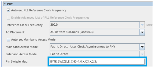
3.3.1.2. Example: Byte Swizzling for x32 LPDDR4 Interface
BL4 and BL5 are not used by LPDDR4 EMIF. The BL0, 1, 6 and 7 are used DQ lanes. Byte lane swapping between BL0 and BL1 is allowed; byte lane swapping between BL6 and BL7 is allowed.
The BYTE_SWIZZLE_CH0 denotes the DQS group implemented in the lane after the swizzling. X indicates that the lane is not used as a data lane (meaning that it serves as an address/command lane or is not used by the EMIF interface).
| Lane Number | BL0 | BL1 | BL2 | BL3 | BL4 | BL5 | BL6 | BL7 |
|---|---|---|---|---|---|---|---|---|
| Default placement | DQ[0] | DQ[1] | AC0 | AC[1] | GPIO | GPIO | DQ[2] | DQ[3] |
| After Byte Swizzling | DQ[1] | DQ[0] | AC0 | AC[1] | GPIO | GPIO | DQ[2] | DQ[3] |
| BYTE SWIZZLE | 1 | 0 | X | X | X | X | 2 | 3 |
To achieve this swizzling, you must enter BYTE_SWIZZLE_CH0=1,0,X,X,X,X,2,3; in the Pin Swizzle Map in the PHY section in the External Memory Interfaces parameter editor.