Visible to Intel only — GUID: dfe1693324304116
Ixiasoft
1. About the External Memory Interfaces Agilex™ 7 M-Series FPGA IP
2. Agilex™ 7 M-Series FPGA EMIF IP – Introduction
3. Agilex™ 7 M-Series FPGA EMIF IP – Product Architecture
4. Agilex™ 7 M-Series FPGA EMIF IP – End-User Signals
5. Agilex™ 7 M-Series FPGA EMIF IP – Simulating Memory IP
6. Agilex™ 7 M-Series FPGA EMIF IP – DDR4 Support
7. Agilex™ 7 M-Series FPGA EMIF IP – DDR5 Support
8. Agilex™ 7 M-Series FPGA EMIF IP – LPDDR5 Support
9. Agilex™ 7 M-Series FPGA EMIF IP – Timing Closure
10. Agilex™ 7 M-Series FPGA EMIF IP – Controller Optimization
11. Agilex™ 7 M-Series FPGA EMIF IP – Debugging
12. Document Revision History for External Memory Interfaces Agilex™ 7 M-Series FPGA IP User Guide
3.1.1. Agilex™ 7 M-Series EMIF Architecture: I/O Subsystem
3.1.2. Agilex™ 7 M-Series EMIF Architecture: I/O SSM
3.1.3. Agilex™ 7 M-Series EMIF Architecture: I/O Bank
3.1.4. Agilex™ 7 M-Series EMIF Architecture: I/O Lane
3.1.5. Agilex™ 7 M-Series EMIF Architecture: Input DQS Clock Tree
3.1.6. Agilex™ 7 M-Series EMIF Architecture: PHY Clock Tree
3.1.7. Agilex™ 7 M-Series EMIF Architecture: PLL Reference Clock Networks
3.1.8. Agilex™ 7 M-Series EMIF Architecture: Clock Phase Alignment
3.1.9. User Clock in Different Core Access Modes
6.2.4.1. Address and Command Pin Placement for DDR4
6.2.4.2. DDR4 Data Width Mapping
6.2.4.3. General Guidelines - DDR4
6.2.4.4. x4 DIMM Implementation
6.2.4.5. Specific Pin Connection Requirements
6.2.4.6. Command and Address Signals
6.2.4.7. Clock Signals
6.2.4.8. Data, Data Strobes, DM/DBI, and Optional ECC Signals
6.3.5.1. Single Rank x 8 Discrete (Component) Topology
6.3.5.2. Single Rank x 16 Discrete (Component) Topology
6.3.5.3. ADDR/CMD Reference Voltage/RESET Signal Routing Guidelines for Single Rank x 8 and Single Rank x 16 Discrete (Component) Topologies
6.3.5.4. Skew Matching Guidelines for DDR4 Discrete Configurations
6.3.5.5. Power Delivery Recommendations for DDR4 Discrete Configurations
6.3.5.6. Agilex™ 7 M-Series EMIF Pin Swapping Guidelines
7.3.1. PCB Stack-up and Design Considerations
7.3.2. General Design Considerations
7.3.3. DDR Differential Signals Routing
7.3.4. Ground Plane and Return Path
7.3.5. RDIMM, UDIMM, and SODIMM Break-in Layout Guidelines
7.3.6. DRAM Break-in Layout Guidelines
7.3.7. DDR5 PCB Layout Guidelines
7.3.8. DDR5 Simulation Strategy
7.3.7.1. DDR5 Discrete Component/Memory Down Topology: up to 40-Bit Interface (1 Rank x8 or x16, 2 Rank x8 or x16)
7.3.7.2. Routing Guidelines for DDR5 Memory Down: 1 Rank or 2 Rank (x8 bit or x16 bit) Configurations
7.3.7.3. Routing Guidelines for DDR5 RDIMM, UDIMM, and SODIMM Configurations
7.3.7.4. Example of a DDR5 layout on Intel FPGA Platform Board
11.1. Interface Configuration Performance Issues
11.2. Functional Issue Evaluation
11.3. Timing Issue Characteristics
11.4. Verifying Memory IP Using the Signal Tap Logic Analyzer
11.5. Debugging with the External Memory Interface Debug Toolkit
11.6. Generating Traffic with the Test Engine IP
11.7. Guidelines for Developing HDL for Traffic Generator
Visible to Intel only — GUID: dfe1693324304116
Ixiasoft
8.3.6.2. Supported LPDDR5 Topologies
The figures in this topic show various supported LPDDR5 topologies, based on the type of DRAM component, number of supported channels, and ranks.
Figure 64. Dual-Channel Single-Rank x16, Dual-Die DRAM Component
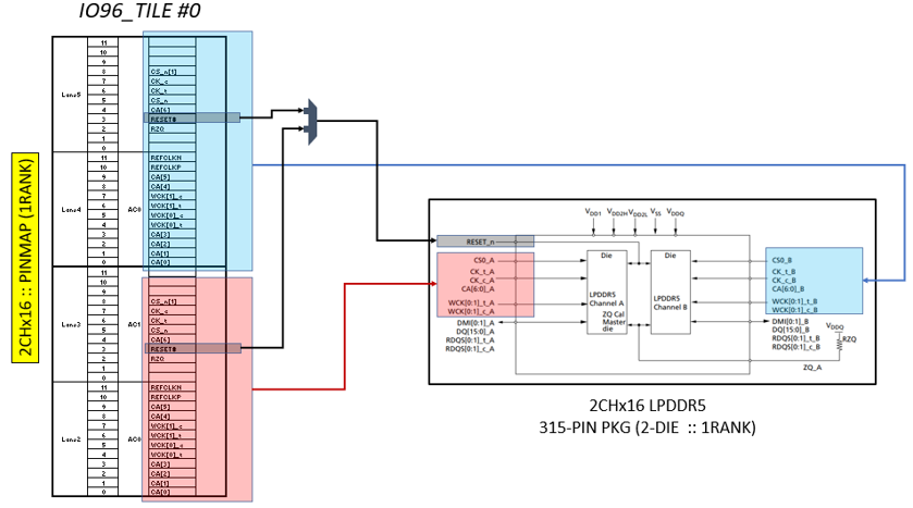
In the above figure, all signals from the controller to DRAM package are point-to-point connections.
Figure 65. Dual-Channel Dual-Rank x16, Using Quad-die DRAM Component
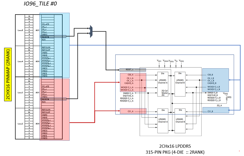
In the above figure, all signals from the controller to DRAM package are point-to-point connections.
Figure 66. Single-Channel Single-Rank x32, Using Dual-die DRAM Component
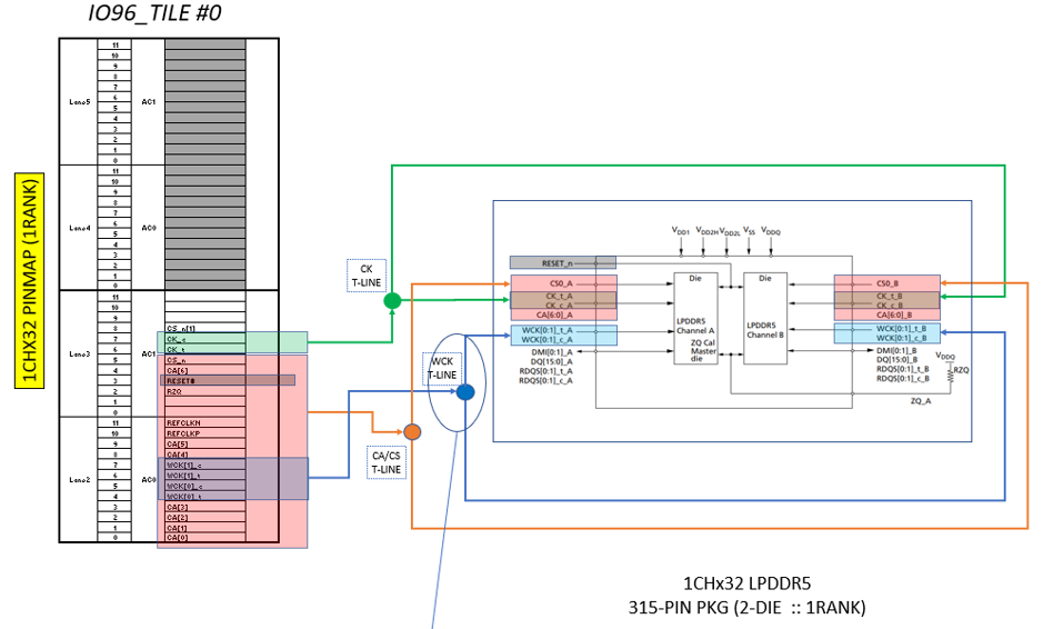
In the above figure, CK, WCK and CA/CS signals from the controller to DRAM are via T-Line connection; each WCK signal from the controller can be connected to both DRAM dies via T-Line, or can be connected to both WCK signals at each DRAM die via T-line.
Figure 67. Single-Channel Dual-Rank x32, Using a Quad-die DRAM component
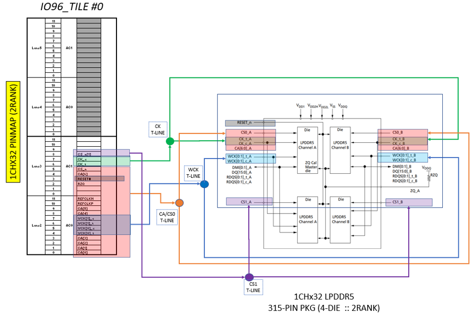
In the above figure, CK, WCK and CA/CS signals from the controller to DRAM are via T-Line connection.
Figure 68. Dual-Channel Single Rank x16, Using a dual-die DRAM Component
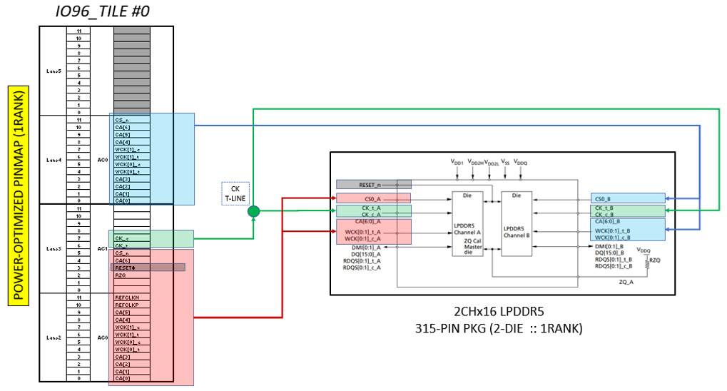
In the above figure, all signals from the controller to DRAM package are point to point connections, except the CK signal which is connected via T-Line in power mode optimization.
Figure 69. Quad-Channel Single Rank x16, Using a Quad-Die DRAM Component
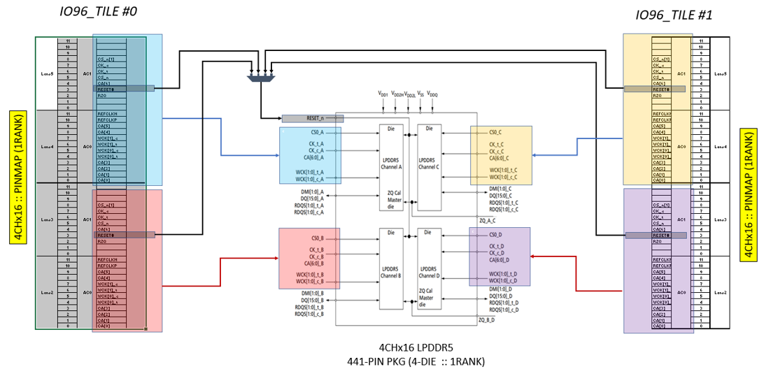
In the above figure, all signals from the controller to DRAM package are point-to-point connections
Figure 70. Quad-Channel Dual-Rank x16, Using an 8-die DRAM Component
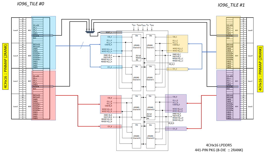
In the above figure, all signals from the controller to DRAM package are point-to-point connections.
Figure 71. Dual-Channel-Single -Rank x32, Using a Quad-Die DRAM Component
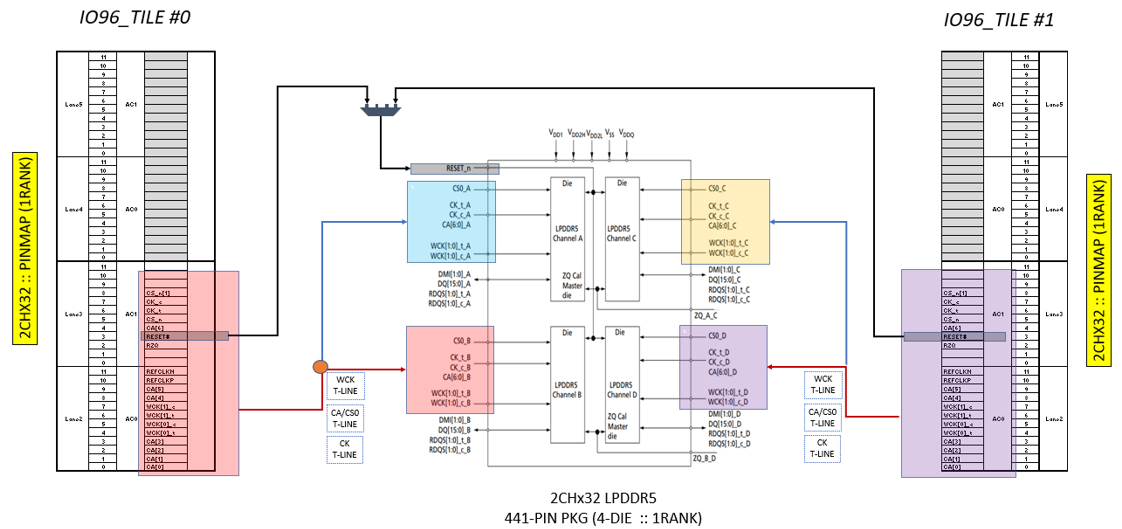
In the above figure, CK, WCK and CA/CS signals are connected to both DRAM dies via T-Line connection.
The following table provides comprehensive routing guidelines (recommended trace impedance and length) for each LPDDR5 signal, based on a memory down topology. For example, the maximum length of the main trace routing can be derived from total trace length by subtracting the break-out and break-in trace segment lengths.
The signal trace width, and minimum spacing/gaps (in mils) from edge-to-edge of signal traces are based on the default stackup shown in the PCB Stack-up and Design Considerations topic; however, PCB designers can use the target impedance for any other stackups. The h value in the table represents the minimum substrate height from signal layer to reference layer.
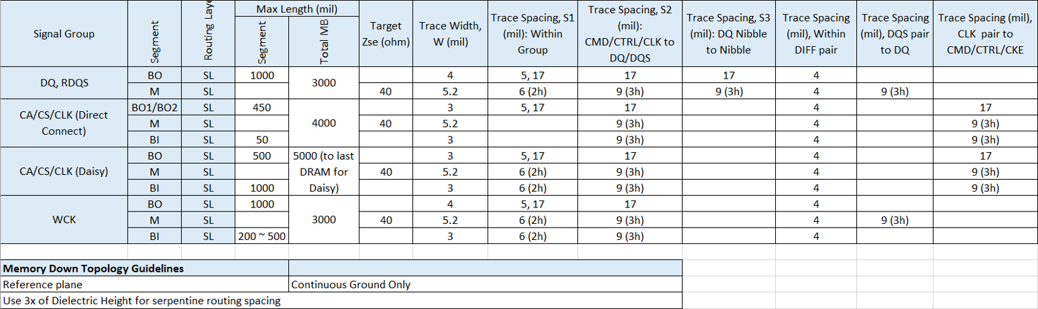
|
Reset signal routing design also follows the CMD/ADD/CTRL routing design. Maintain at least 5x h edge-to-edge spacing from the Reset signal to other signals on the same layer. There is no requirement to have skew matching between Reset signal and CLK signal.
Skew matching for the LPDDR5 interface consists of both package routing skew and PCB physical routing skew. You must maintain skew matching of CA and CTRL with respect to the clock signals to ensure signals at the receiver are correctly sampled. In addition, there are skew matching requirements for DQ and DQS within a byte group, DQS and CLK.
The following table provides a detailed skew matching guideline to facilitate PCB trace routing efforts. The length matching criteria in the table below represents a default PCB on an Intel platform board design. Skew matching criteria must be always followed in any other stackup.
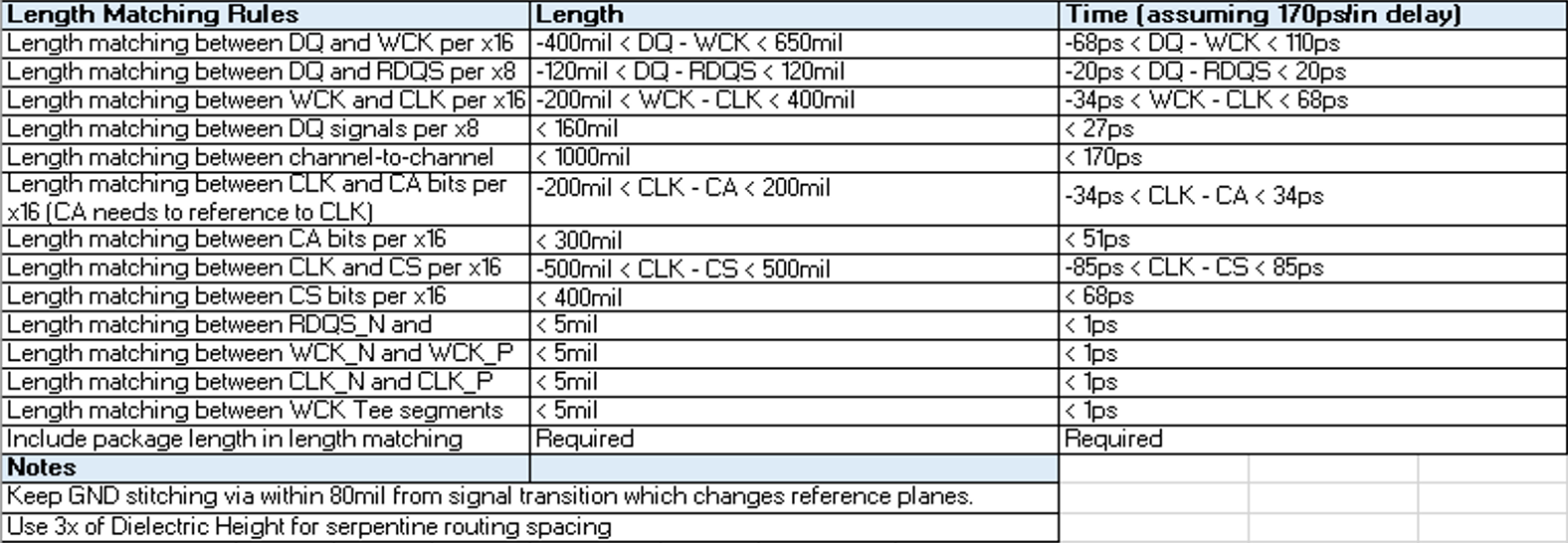
|
LPDDR5 eye margin is sensitive to crosstalk, especially when the signals are routed on deep layers in the stackup. The deep-layer vertical transition induces more vertical coupling between signals and hence more crosstalk.
Intel recommends keeping the via transition depth in Z-direction to less than 16mil (routed on shallow layers with backdrill) to achieve high performance on the LPDDR5 interface. The maximum data rate of LPDDR5 depends on the type of PCB and on the DDR memory down configuration as seen in the following table.
| Memory | LPDDR5 | |
|---|---|---|
| Signal; Group | DQ | |
| Board Thickness (mil) | 65mil or 120mil (Routing must be on upper layers, max via transition depth <=16mil) | 65mil or 120mil (Routing must be on upper layers, max via transition depth <=16mil) |
| Maximum Z-transition height (mil) | 16 | 16 |
| PCB Stripline Trace Impedance (Ohms) | 40 | 40 |
| Memory Configuration | Memory Down | Memory Down |
| # of Rank | 1 (x16 bit or x32 bit Double Die) | 2 (x 16 or x 32 bit) |
| Maximum Length Total (Inch) | 3.0 | 3.0 |
| Notes | Maximum package length in FPGA design is shorter than 34mm. | |