Visible to Intel only — GUID: luy1693244616234
Ixiasoft
1. About the External Memory Interfaces Agilex™ 7 M-Series FPGA IP
2. Agilex™ 7 M-Series FPGA EMIF IP – Introduction
3. Agilex™ 7 M-Series FPGA EMIF IP – Product Architecture
4. Agilex™ 7 M-Series FPGA EMIF IP – End-User Signals
5. Agilex™ 7 M-Series FPGA EMIF IP – Simulating Memory IP
6. Agilex™ 7 M-Series FPGA EMIF IP – DDR4 Support
7. Agilex™ 7 M-Series FPGA EMIF IP – DDR5 Support
8. Agilex™ 7 M-Series FPGA EMIF IP – LPDDR5 Support
9. Agilex™ 7 M-Series FPGA EMIF IP – Timing Closure
10. Agilex™ 7 M-Series FPGA EMIF IP – Controller Optimization
11. Agilex™ 7 M-Series FPGA EMIF IP – Debugging
12. Document Revision History for External Memory Interfaces Agilex™ 7 M-Series FPGA IP User Guide
3.1.1. Agilex™ 7 M-Series EMIF Architecture: I/O Subsystem
3.1.2. Agilex™ 7 M-Series EMIF Architecture: I/O SSM
3.1.3. Agilex™ 7 M-Series EMIF Architecture: I/O Bank
3.1.4. Agilex™ 7 M-Series EMIF Architecture: I/O Lane
3.1.5. Agilex™ 7 M-Series EMIF Architecture: Input DQS Clock Tree
3.1.6. Agilex™ 7 M-Series EMIF Architecture: PHY Clock Tree
3.1.7. Agilex™ 7 M-Series EMIF Architecture: PLL Reference Clock Networks
3.1.8. Agilex™ 7 M-Series EMIF Architecture: Clock Phase Alignment
3.1.9. User Clock in Different Core Access Modes
6.2.4.1. Address and Command Pin Placement for DDR4
6.2.4.2. DDR4 Data Width Mapping
6.2.4.3. General Guidelines - DDR4
6.2.4.4. x4 DIMM Implementation
6.2.4.5. Specific Pin Connection Requirements
6.2.4.6. Command and Address Signals
6.2.4.7. Clock Signals
6.2.4.8. Data, Data Strobes, DM/DBI, and Optional ECC Signals
6.3.5.1. Single Rank x 8 Discrete (Component) Topology
6.3.5.2. Single Rank x 16 Discrete (Component) Topology
6.3.5.3. ADDR/CMD Reference Voltage/RESET Signal Routing Guidelines for Single Rank x 8 and Single Rank x 16 Discrete (Component) Topologies
6.3.5.4. Skew Matching Guidelines for DDR4 Discrete Configurations
6.3.5.5. Power Delivery Recommendations for DDR4 Discrete Configurations
6.3.5.6. Agilex™ 7 M-Series EMIF Pin Swapping Guidelines
7.3.1. PCB Stack-up and Design Considerations
7.3.2. General Design Considerations
7.3.3. DDR Differential Signals Routing
7.3.4. Ground Plane and Return Path
7.3.5. RDIMM, UDIMM, and SODIMM Break-in Layout Guidelines
7.3.6. DRAM Break-in Layout Guidelines
7.3.7. DDR5 PCB Layout Guidelines
7.3.8. DDR5 Simulation Strategy
7.3.7.1. DDR5 Discrete Component/Memory Down Topology: up to 40-Bit Interface (1 Rank x8 or x16, 2 Rank x8 or x16)
7.3.7.2. Routing Guidelines for DDR5 Memory Down: 1 Rank or 2 Rank (x8 bit or x16 bit) Configurations
7.3.7.3. Routing Guidelines for DDR5 RDIMM, UDIMM, and SODIMM Configurations
7.3.7.4. Example of a DDR5 layout on Intel FPGA Platform Board
11.1. Interface Configuration Performance Issues
11.2. Functional Issue Evaluation
11.3. Timing Issue Characteristics
11.4. Verifying Memory IP Using the Signal Tap Logic Analyzer
11.5. Debugging with the External Memory Interface Debug Toolkit
11.6. Generating Traffic with the Test Engine IP
11.7. Guidelines for Developing HDL for Traffic Generator
Visible to Intel only — GUID: luy1693244616234
Ixiasoft
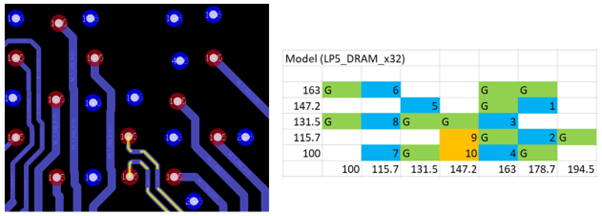
8.3.6.3. Example of an LPDDR5 Layout on an Intel® FPGA Platform Board
The following figures show the layout example of a single rank LPDDR5 x 32-bit device with a pitch size of 0.7×0.8mm on an Intel FPGA platform design.
This example has been designed on a thick PCB (120mil stackup) using micro vias and through vias with backdrill. The LPDDR5 signal routing is on upper layers to avoid vertical crosstalk on interface and achieve high performance.
Figure 72. Board Layout and Via Pattern for Single Rank LPDDR5 x32 device on an Intel FPGA Platform Design
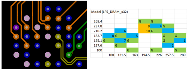
In addition, the following figure shows a LPDDR5 64-bit device board routing sample with pitch dimension of 0.4×0.4mm. The microvia has been used for via transitions on this interface.
Figure 73. Board Via Pattern for LPDDR5 64-bit Device