Visible to Intel only — GUID: juv1654713058660
Ixiasoft
1. Three-phase Boost Bidirectional AC/DC Converter for Electric Vehicle (EV) Charging Design Example Overview
2. Downloading and Installing the Design Example
3. Model Description
4. FPGA Resource Use Comparison
5. Locating Top-level VHDL Wrapper
6. Generating HDL Code with MATLAB and HDL Coder
7. Simulink Simulation Results
8. Document Revision History for AN 973: Three-phase Boost Bidirectional AC/DC Converter for EV Charging
Visible to Intel only — GUID: juv1654713058660
Ixiasoft
2.3. Downloading and Installing the Design
Perform the following steps to download and install the Three-phase Boost Bidirectional AC/DC Converter for EV Charging design example:
Note: The Three-phase Boost Bidirectional AC/DC Converter for EV Charging design example includes a precompiled .sof in the master_image directory.
- Download the relevant design .par file for your development kit and power board from the Intel FPGA Design Store.
The file you downloaded is in the form of a <project>.par file, which contains a compressed version of the design example (similar to a .qar file) and metadata describing the project. The combination of this information is what constitutes a <project>.par file.
- In the Intel® Quartus® Prime software, click File > New Project Wizard. The New Project Wizard dialog box launches with the Introduction screen.
- Click Next. The Directory, Name, Top-Level Entity screen displays.
- Enter the path for your project working directory.
- Specify a project name.
- Click Next. The Project Type screen displays.
- Select Project template.
- Click Next. The Design Templates screen displays.
- Click the Install the design templates link. The Design Template Installation dialog box appears.
- In the Design template file (.par) field, browse to select the .par file of the design example and browse to the destination directory (optional) where you want to install it.
- Click OK. The design template installation success message appears.
- Click OK.
- Select the Three-phase Boost Bidirectional AC/DC Converter for EV Charging design example.
- Click Next. The Summary screen appears.
- Click Finish. The Intel® Quartus® Prime software expands the archive and sets up the project, which may take some time.
- Click Processing > Start Compilation.
- Connect the relevant USB cable from the USB connector on the development board to your computer.
- J12 for Intel® MAX® 10 FPGA Development Kit
- J37 for Cyclone® V SoC Development Kit
- Supply power to the development board.
- After compilation ends, click Tools > Programmer to program your Intel® MAX® 10 Development Kit or Cyclone® V SoC Development Kit. Use the Auto Detect feature if necessary.
- Select the master_image/bidir_rectifier_fixed_quartus.sof file or your newly generated output_files/bidir_rectifier_fixed_quartus.sof file.
Note: The Programming the Board figure shows the programmer for Cyclone® V SoC Development Kit FPGA (5CSXFC6D6F31).
- Select the Program/Configure check box in the table.
- Click Start. The Progress bar displays in green a 100% (Successful) legend.
Figure 4. Programming the Board
- Return to the Intel® Quartus® Prime software and click Tools > Signal Tap logic analyzer.
- In the Signal Tap logic analyzer window, in the top right corner, click Setup to select USB-BlasterII as shown in Hardware Setup.
- Select the appropriate FPGA device.
- Intel® MAX® 10 Development Kit: Select @1: 10M50DA(.ES)/10M50DC (0x031050DD)
- Cyclone® V SoC Development Kit: Select @2: 5CSEBA6(.ES)/5CSEMA6/..(0x02D020DD.
Figure 5. Hardware Setup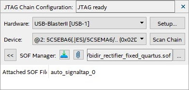
- In the Signal Tap logic analyzer window, select the Data tab and click
 . The following image shows the waveform:
Figure 6. Signal Tap Logic Analyzer Waveform
. The following image shows the waveform:
Figure 6. Signal Tap Logic Analyzer Waveform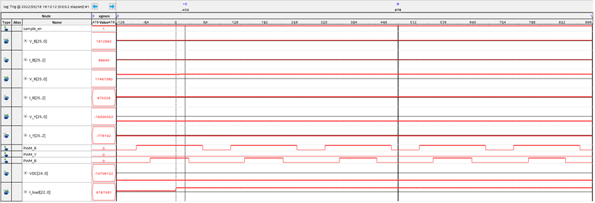
- Navigate to the matlab/Simulink directory and double-click the run_stp_control.bat file to adjust the sampling resolution.
- In the EV Charger dialog box, set the values of VDC Offset (V) to -800 and Signaltap Sample period (clks) to 8191 as shown in the following image:
Figure 7. Changing VDC Offset and Signaltap Sample Period
- Return to the Signal Tap logic analyzer window and click . The view updates as shown in the following images:
Figure 8. Scaled Output Waveform in the Signal Tap Logic Analyzer
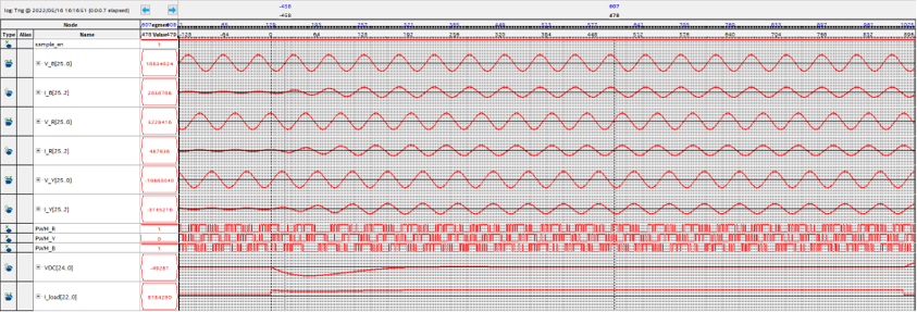 The following are waveform components' details:
- In the model, the output DC Voltage (VDC) is regulated to 800V. Setting the VDC Offset to -800 V allows the maximum range to be easily visible in the Signal Tap logic analyzer.
- The SignalTap Sample Period sets the period of a counter, which enables waveforms sampling. A value of n results in samples every n-1 clock cycles. So, a value of 0 samples every clock cycle results in no aliasing with a very short visible period. The value of 8191 is shown in step 28 samples every 8192 cycles, so the Pulse Width Modulation (PWM) signals are highly aliased, but a long time frame becomes visible.
You can run the GUI script from the Intel® Quartus® Prime software TCL console with the following command:exec quartus_stp -t ../../stp_control.tcl &
Note: The ../../ path depends on the current directory of the Intel® Quartus® Prime software.