DSP Builder Model Description for the DC-DC Converter Design Example
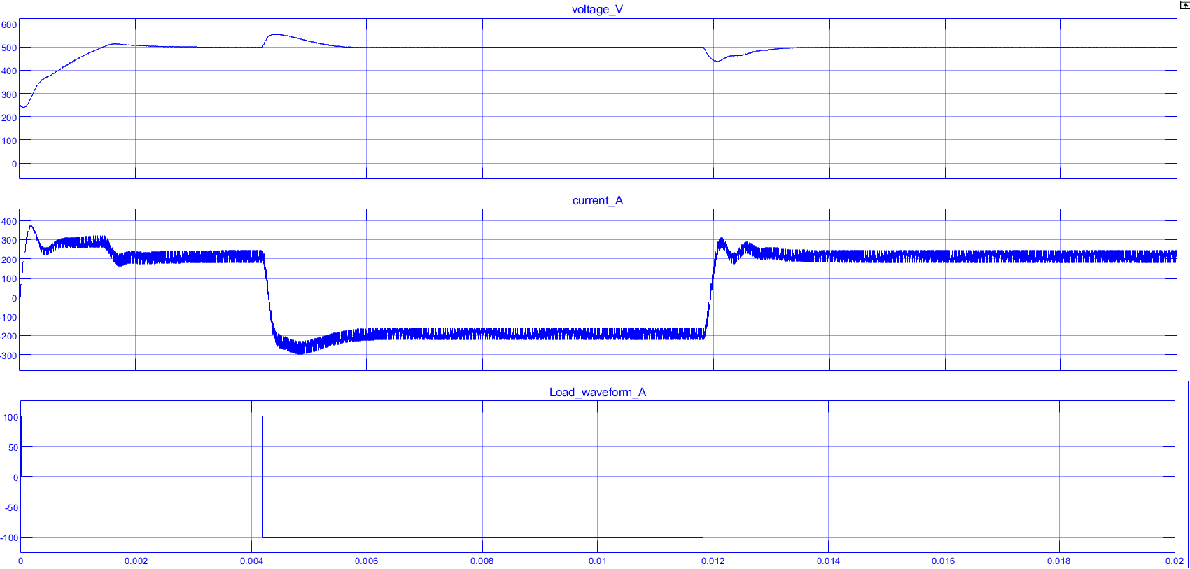
The complete system can run in real-time on one FPGA. The load current is simulated as a square waveform with positive and negative values, which in turn generates current and voltage waveforms inside the DC-DC converter. When the load current switches, the transient current and voltage signals can be examined either at the output of DAC on the Intel MAX 10 development board with an external oscilloscope or using the SignalTap II Logic Analyzer file (stp1_voltagecurrent_waveform.stp) within Intel Quartus Prime on a computer.


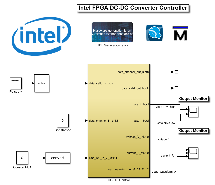
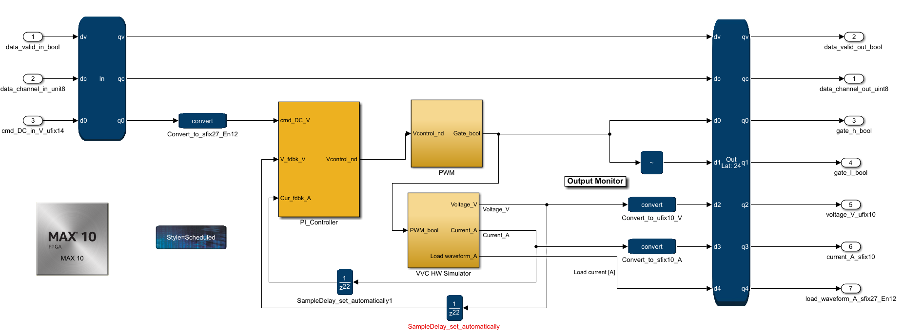
The DC-DC Control block has the portion of the simulation for which VHDL code is generated. The ChannelIn and ChannelOut blocks are the port interface for the VHDL code. The MATLAB Simulink inport and outport signals define the VHDL signal names, and the VHDL data formats are the signal formats that you typically set with the Convert block.

PI controller
The PI controller includes one current control loop and one voltage control loop. For more information on the controller and tuning, refer to in the FPGA-Based Control for Electric Vehicle and Hybrid Electric Vehicle Power Electronics White Paper.
PWM: Pulse Width Modulation
In the PWM block, the design generates a triangular wave bounded within [-1.1] using an SR latch and counter counting at the frequency of the system clock of 100 MHz. Each step size is:
Step size = f PWM x 4 x t clock = 0.002
where:
f PWM is the sampling frequency, which is 50 kHz in this design. t clock is the period of the system clock. The system clock runs at 100 MHz, which is 10 ns.
After every 2/(step size) steps, the counter changes the direction of up-down counting. The design compares the triangular signal with current control signals bounded within [-0.9, 0.9] to produce pulses for driving gates for each phase.
VCC Hardware Simulator
The DC-DC converter is simply modelled as functions of gate driving signals and input (battery) voltage in the forms of Simulink math or logic operation blocks. The output current is:
I a/b = (V battery – not_PWM a/b × V out ) × 1/L × 1/S
The output voltage is:
V out = V c = (I a × not_PWM a + I b × not_PWM b – I load × H LPF ) × 1/C × 1/S
I load is a prespecified waveform and H LPF is the transfer function of a low pass filter with a 1.6 kHz cut-off frequency.