AN 777: Data Word Alignment Calibration With Multiple Intel FPGA PHYLite for Parallel Interfaces IP Cores
ID
683631
Date
1/12/2018
Public
Visible to Intel only — GUID: ppd1478239084252
Ixiasoft
1.1. Features
1.2. Hardware and Software Requirements
1.3. Compiling the Reference Design
1.4. Hardware Setup
1.5. Generating Executable and Linking Format (.elf) Programming File
1.6. Running the Hardware Reference Design
1.7. Results
1.8. Reference Design Architecture
1.9. Document Revision History for AN 777: Data Word Alignment Calibration With Multiple Intel FPGA PHYLite for Parallel Interfaces IP Cores
Visible to Intel only — GUID: ppd1478239084252
Ixiasoft
1.4. Hardware Setup
The following steps are to setup the Intel® Arria® 10 FPGA development kit before running the reference design.
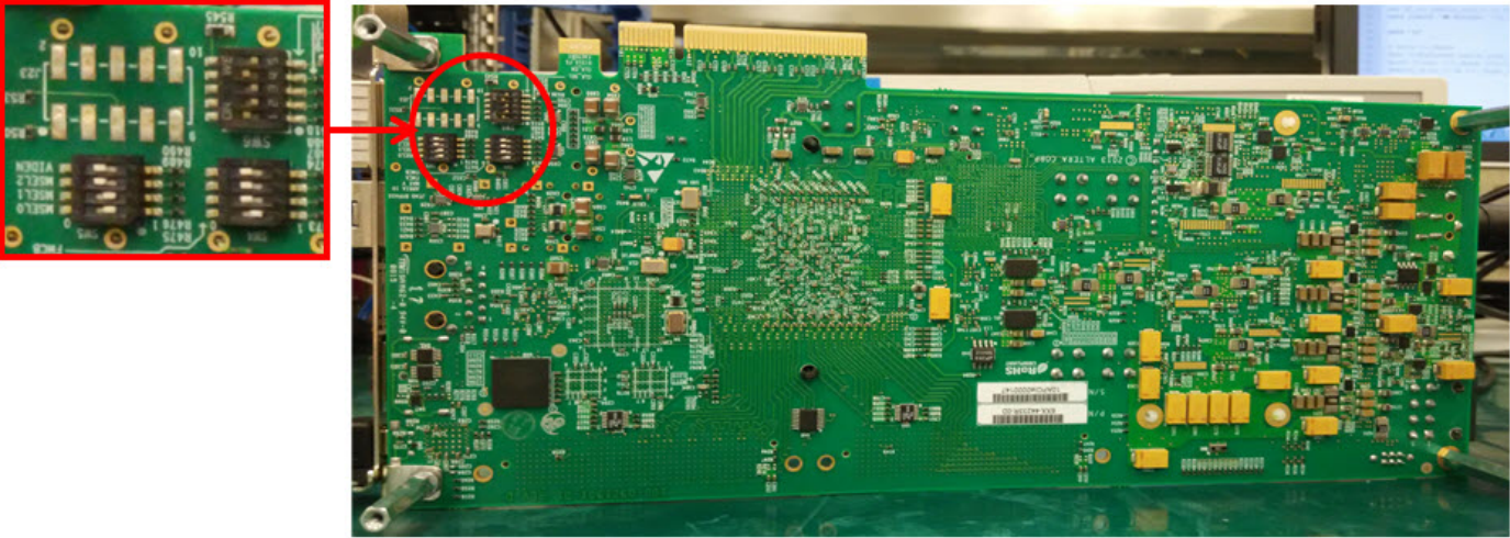
- Set the Intel® Arria® 10 FPGA development board switches to according to the following figure.
Figure 6. Intel® Arria® 10 FPGA Development Board Switch Settings

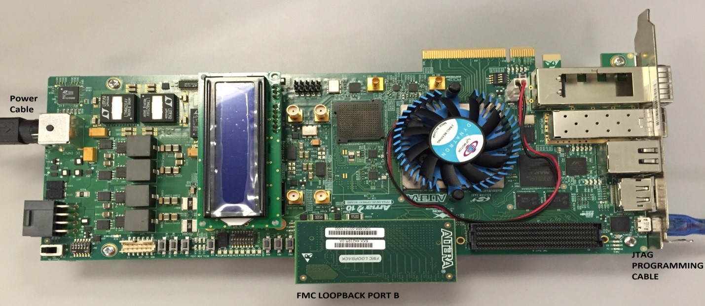
- Connect the loopback FPGA mezzanine (FMC) daughter card on the FMC loopback Port B.
Figure 7. Connection for Loopback FPGA Mezzanine (FMC) Daughter Card

- Connect the Intel® FPGA Download Cable to the Intel® Arria® 10 FPGA development kit and your host machine.
- Click Tools -> Programmer to program the <project directory> /master_image/top.sof file into the Arria 10 FPGA development board.