Visible to Intel only — GUID: mtr1422491942493
Ixiasoft
1. Introduction to Intel® FPGA Design Flow for AMD* Xilinx* Users
2. Technology Comparison
3. FPGA Tools Comparison
4. AMD* Xilinx* to Intel® FPGA Design Conversion
5. Conclusion
6. AN 307: Intel® FPGA Design Flow for AMD* Xilinx* Users Archives
7. Document Revision History for Intel® FPGA Design Flow for AMD* Xilinx* Users
3.3.1. Project Creation
3.3.2. Design Entry
3.3.3. IP Status
3.3.4. Design Constraints
3.3.5. Synthesis
3.3.6. Design Implementation
3.3.7. Finalize Pinout
3.3.8. Viewing and Editing Design Placement
3.3.9. Static Timing Analysis
3.3.10. Generation of Device Programming Files
3.3.11. Power Analysis
3.3.12. Simulation
3.3.13. Hardware Verification
3.3.14. View Netlist
3.3.15. Design Optimization
3.3.16. Techniques to Improve Productivity
3.3.17. Partial Reconfiguration
3.3.18. Cross-Probing in the Quartus® Prime Pro Edition Software
4.2.1.2.1. Memory Mode
4.2.1.2.2. Clocking Mode
4.2.1.2.3. Write and Read Operation Triggering
4.2.1.2.4. Read-During-Write Operation at the Same Address
4.2.1.2.5. Error Correction Code (ECC)
4.2.1.2.6. Byte Enable
4.2.1.2.7. Address Clock Enable
4.2.1.2.8. Parity Bit Support
4.2.1.2.9. Memory Initialization
4.2.1.2.10. Output Synchronous Set/Reset
Visible to Intel only — GUID: mtr1422491942493
Ixiasoft
3.3.2.2. Schematic/Block Editor
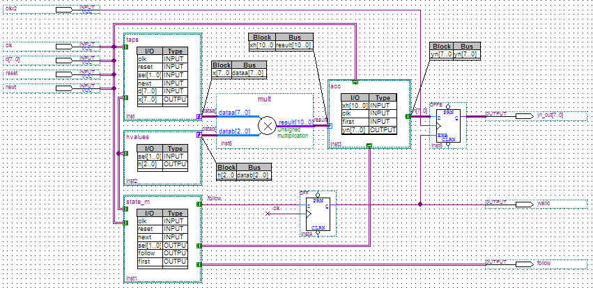
In the Quartus® Prime Pro Edition software, you can use Intel® FPGA-supplied design elements, such as Boolean gates and registers, or you can create your own symbols from HDL or EDA netlist design entities.
- To create a block design file from a VHDL or Verilog HDL design file, click File > Create/Update, and click Create Symbol Files for Current File.
- To create a new schematic file (*.bdf) in the Quartus® Prime Pro Edition software, point to File > New and select the Block Diagram/Schematic File.
- To insert block symbols into the schematic, double-click the schematic file and choose the appropriate block symbols.
Figure 3. Schematic File

